如果你也在 怎样代写数字信号处理digital signal process这个学科遇到相关的难题,请随时右上角联系我们的24/7代写客服。数字信号处理digital signal process是指使用数字处理,如通过计算机或更专业的数字信号处理器,来进行各种信号处理操作。以这种方式处理的数字信号是一连串的数字,代表时间、空间或频率等领域中连续变量的样本。在数字电子学中,数字信号被表示为脉冲序列,它通常由晶体管的开关产生。
数字信号处理digital signal process和模拟信号处理是信号处理的子领域。DSP的应用包括音频和语音处理、声纳、雷达和其他传感器阵列处理、频谱密度估计、统计信号处理、数字图像处理、数据压缩、视频编码、音频编码、图像压缩、电信的信号处理、控制系统、生物医学工程和地震学等。
my-assignmentexpert™ 数字信号处理digital signal process作业代写,免费提交作业要求, 满意后付款,成绩80\%以下全额退款,安全省心无顾虑。专业硕 博写手团队,所有订单可靠准时,保证 100% 原创。my-assignmentexpert™, 最高质量的数字信号处理digital signal process作业代写,服务覆盖北美、欧洲、澳洲等 国家。 在代写价格方面,考虑到同学们的经济条件,在保障代写质量的前提下,我们为客户提供最合理的价格。 由于统计Statistics作业种类很多,同时其中的大部分作业在字数上都没有具体要求,因此数字信号处理digital signal process作业代写的价格不固定。通常在经济学专家查看完作业要求之后会给出报价。作业难度和截止日期对价格也有很大的影响。
想知道您作业确定的价格吗? 免费下单以相关学科的专家能了解具体的要求之后在1-3个小时就提出价格。专家的 报价比上列的价格能便宜好几倍。
my-assignmentexpert™ 为您的留学生涯保驾护航 在信息Information作业代写方面已经树立了自己的口碑, 保证靠谱, 高质且原创的数字信号处理digital signal process代写服务。我们的专家在信息Information代写方面经验极为丰富,各种数字信号处理digital signal process相关的作业也就用不着 说。
我们提供的数字信号处理digital signal process及其相关学科的代写,服务范围广, 其中包括但不限于:
调和函数 harmonic function
椭圆方程 elliptic equation
抛物方程 Parabolic equation
双曲方程 Hyperbolic equation
非线性方法 nonlinear method
变分法 Calculus of Variations
几何分析 geometric analysis
偏微分方程数值解 Numerical solution of partial differential equations
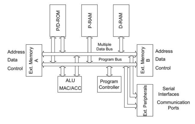
信号代写|数字信号处理作业代写digital signal process代考|Fixed-point DSPs
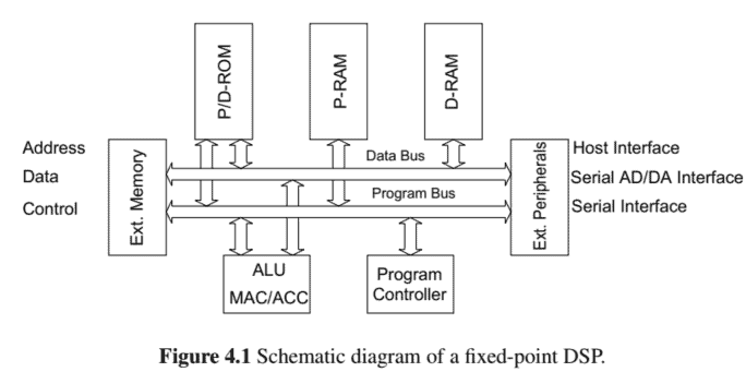
The discrete-time and discrete-amplitude output of an AD converter is usually represented in 2’s complement format. The processing of these number sequences is carried out with fixed-point or floating-point arithmetic. The output of a processed signal is again in 2’s complement format and is fed to a DA converter. The signed fractional representation (2’s complement) is the common method for algorithms in fixed-point number representation. For address generation and modulo operations unsigned integers are used. Figure $4.1$ shows a schematic diagram of a typical fixed-point DSP. The main building blocks are program controller, arithmetic logic unit (ALU) with a multiplier-accumulator (MAC), program and data memory and interfaces to external memory and peripherals. All blocks are connected with each other by an internal bus system. The internal bus system has separate instruction and data buses. The data bus itself can consist of more than one parallel bus enabling it, for instance, to transmit both operands of a multiplication instruction to the MAC in parallel. The internal memory consists of instruction and data RAM and additional ROM memory. This internal memory permits fast execution of internal instructions and data transfer. For increasing memory space, address/control and data buses are connected to external memories like EPROM, ROM and RAM. The connection of the external bus system to the internal bus architecture has great influence on efficient execution of external instructions as well as on processing external data. In order to connect serially operating AD/DA converters, special serial interfaces with high transmission rates are offered by several DSPs. Moreover, some processors support direct connection to an RS232 interface. The control from a microprocessor can be achieved via a host interface with a word-length of 8 bits.
信号代写|数字信号处理作业代写digital signal process代考|Floating-point DSPs
Figure $4.2$ shows the block diagram of a typical floating-point DSP. The main characteristics of the different architectures are the dual-port principle (Motorola, Texas Instruments) and the external Harvard architecture (Analog Devices, NEC). Floating-point DSPs internally have multiple bus systems in order to accelerate data transfer to the processing unit. An on-chip DMA controller and cache memory support higher data transfer rates. An overview of floating-point DSPs is shown in Table 4.3. Besides the standardized floatingpoint representation IEEE-754, there are also manufacturer-dependent number representations.
信号代写|数字信号处理作业代写digital signal process代考|Weighted Resistors and Capacitors
A reduction in the number of identical resistors or current sources is achieved with the following method.
Weighted Resistors. DA conversion with $w$ switched current sources which are weighted according to
$$
I_{1}=2 I_{2}=4 I_{3}=\cdots=2^{w-1} I_{w}
$$
is shown in Fig. 3.45. The output voltage is
$$
U_{2}=-R \cdot I=-R \cdot\left(b_{1} I_{1} 2^{0}+b_{2} I_{2} 2^{1}+b_{3} I_{3} 2^{2}+\cdots+b_{w} I_{w} 2^{w-1}\right)
$$
where $b_{n}$ takes values 0 or 1 . The implementation of DA conversion with switched current sources is carried out with weighted resistors as shown in Fig. 3.46. The output voltage is
$$
\begin{aligned}
U_{2} &=R \cdot I=R\left(\frac{b_{1}}{2 R}+\frac{b_{2}}{4 R}+\frac{b_{4}}{8 R}+\cdots+\frac{b_{w}}{2^{w} R}\right) U_{R} \
&=\left(b_{1} 2^{-1}+b_{2} 2^{-2}+b_{3} 2^{-3}+\cdots+b_{w} 2^{-w}\right) U_{R}
\end{aligned}
$$
数字信号处理代写
信号代写|数字信号处理作业代写DIGITAL SIGNAL PROCESS代考|FIXED-POINT DSPS
AD 转换器的离散时间和离散幅度输出通常以 2 的补码格式表示。这些数字序列的处理是通过定点或浮点运算进行的。已处理信号的输出再次采用 2 的补码格式,并馈送到 DA 转换器。有符号小数表示2′sC这米pl和米和n吨是定点数表示中算法的常用方法。对于地址生成和模运算,使用无符号整数。数字4.1显示了一个典型的定点DSP的示意图。主要构建块是程序控制器、算术逻辑单元一种大号在带有乘法累加器米一种C、程序和数据存储器以及与外部存储器和外围设备的接口。所有块通过内部总线系统相互连接。内部总线系统具有独立的指令和数据总线。数据总线本身可以由多个并行总线组成,例如,可以将乘法指令的两个操作数并行传输到 MAC。内部存储器由指令和数据 RAM 以及附加的 ROM 存储器组成。该内部存储器允许快速执行内部指令和数据传输。为了增加存储空间,地址/控制和数据总线连接到外部存储器,如 EPROM、ROM 和 RAM。外部总线系统与内部总线体系结构的连接对外部指令的有效执行以及对外部数据的处理有很大的影响。为了连接串行运行的 AD/DA 转换器,几个 DSP 提供了具有高传输速率的特殊串行接口。此外,一些处理器支持直接连接到 RS232 接口。微处理器的控制可以通过一个字长为 8 位的主机接口来实现。
信号代写|数字信号处理作业代写DIGITAL SIGNAL PROCESS代考|FLOATING-POINT DSPS
数字4.2显示了典型浮点 DSP 的框图。不同架构的主要特点是双端口原理米这吨这r这l一种,吨和X一种s一世ns吨r在米和n吨s和外部哈佛架构一种n一种l这GD和在一世C和s,ñ和C. 浮点 DSP 内部有多个总线系统,以加速向处理单元的数据传输。片上 DMA 控制器和高速缓存支持更高的数据传输速率。浮点 DSP 的概述如表 4.3 所示。除了标准化的浮点表示法 IEEE-754,还有制造商相关的数字表示法。
信号代写|数字信号处理作业代写DIGITAL SIGNAL PROCESS代考|WEIGHTED RESISTORS AND CAPACITORS
使用以下方法可以减少相同电阻器或电流源的数量。
加权电阻。DA转换与在被加权的开关电流源
一世1=2一世2=4一世3=⋯=2在−1一世在
如图 3.45 所示。输出电压为
在2=−R⋅一世=−R⋅(b1一世120+b2一世221+b3一世322+⋯+b在一世在2在−1)
在哪里bn取值 0 或 1 。使用图 3.46 所示的加权电阻器执行开关电流源的 DA 转换。输出电压为
在2=R⋅一世=R(b12R+b24R+b48R+⋯+b在2在R)在R =(b12−1+b22−2+b32−3+⋯+b在2−在)在R

信号代写|数字信号处理作业代写digital signal process代考 请认准UprivateTA™. UprivateTA™为您的留学生涯保驾护航。