如果你也在 怎样代写电路设计Filter Design这个学科遇到相关的难题,请随时右上角联系我们的24/7代写客服。电路设计Filter Design是设计一个满足一系列要求的信号处理滤波器的过程,其中一些要求可能是相互冲突的。其目的是找到一个能充分满足每项要求的滤波器,使其发挥作用。
电路设计Filter Design过程可以被描述为一个优化问题,其中每个要求都有助于一个应该被最小化的误差函数。设计过程的某些部分可以自动化,但通常需要有经验的电气工程师来获得一个好的结果。是一个具有欺骗性的复杂课题。尽管电路设计很容易理解和计算,但其设计和实现的实际挑战是巨大的,是高级研究的主题。
my-assignmentexpert™ 电路设计Filter Design作业代写,免费提交作业要求, 满意后付款,成绩80\%以下全额退款,安全省心无顾虑。专业硕 博写手团队,所有订单可靠准时,保证 100% 原创。my-assignmentexpert™, 最高质量的电路设计Filter Design作业代写,服务覆盖北美、欧洲、澳洲等 国家。 在代写价格方面,考虑到同学们的经济条件,在保障代写质量的前提下,我们为客户提供最合理的价格。 由于统计Statistics作业种类很多,同时其中的大部分作业在字数上都没有具体要求,因此电路设计Filter Design作业代写的价格不固定。通常在经济学专家查看完作业要求之后会给出报价。作业难度和截止日期对价格也有很大的影响。
想知道您作业确定的价格吗? 免费下单以相关学科的专家能了解具体的要求之后在1-3个小时就提出价格。专家的 报价比上列的价格能便宜好几倍。
my-assignmentexpert™ 为您的留学生涯保驾护航 在EE作业代写方面已经树立了自己的口碑, 保证靠谱, 高质且原创的电路设计Filter Design代写服务。我们的专家在EE代写方面经验极为丰富,各种电路设计Filter Design相关的作业也就用不着 说。
我们提供的电路设计Filter Design及其相关学科的代写,服务范围广, 其中包括但不限于:
EE代写|电路设计作业代写Filter Design代考|Voltage Amplification
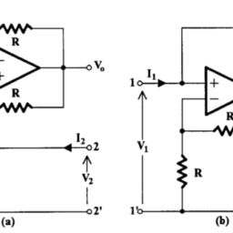
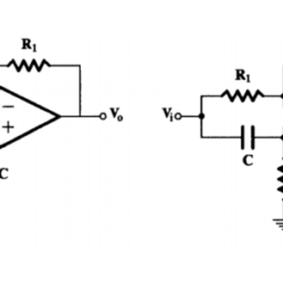
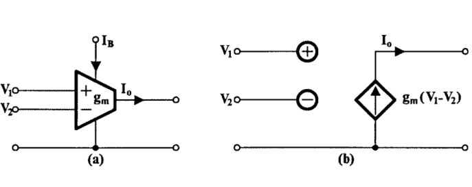
Inverting and noninverting voltage amplification can be achieved using an OTA as shown in Fig. 3.22(a) and 3.22(b), respectively. Any desired gain can be achieved by a proper choice of $g_{m}$ and $R_{L}$. It should be noted that the output voltage $V_{o}$ is obtained from a source with output impedance equal to $R_{L}$. Zero output impedance can be achieved only if such circuits are followed by a buffer or voltage follower.
EE代写|电路设计作业代写Filter Design代考|A Voltage-Variable Resistor (VVR)
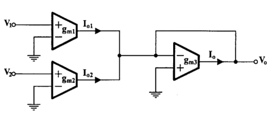
A grounded voltage-variable resistor can be easily obtained using the ideal OTA as shown in Fig. 3.23. Since $I_{o}=-I_{i}$, we will have the following:
$$
Z_{i}=\frac{V_{i}}{I_{i}}=\frac{V_{i}}{-I_{o}}=\frac{V_{i}}{g_{m} V_{i}}=\frac{1}{g_{m}}
$$
Using two such arrangements cross-connected in parallel, a floating VVR can be obtained. On the other hand, if in Fig. $3.23$ the input terminals are interchanged, the input resistance will be $-1 / g_{m}$. Thus, using OTAs, both positive and negative resistors become available without actually having to build them on the chip. These, coupled with capacitors, lead to the creation of the so-called active-C filters discussed later in this book.
EE代写|电路设计作业代写FILTER DESIGN代考|Integration
The operation of integration can be achieved very conveniently using the OTA as is shown in Fig. 3.25. Clearly,
$$
V_{o}=\frac{I_{o}}{s C}=\frac{g_{m}}{s C}\left(V_{1}-V_{2}\right)
$$
It follows that both inverting and noninverting integration is easily achieved. Of course, in all cases, the output impedance of the circuit is nonzero.
If a resistor is connected in parallel with C in Fig. 3.25, the integration will become lossy. On the other hand, connecting the circuit in Fig. $3.23$ at the output of that in Fig. 3.25, the integration becomes both lossy and adjustable.
电路设计代写
E代写|电路设计作业代写FILTER DESIGN代考|VOLTAGE AMPLIFICATION
可以使用 OTA 实现反相和同相电压放大,如图 3.22 所示一种和 3.22b, 分别。任何所需的增益都可以通过适当的选择来实现G米和R大号. 需要注意的是,输出电压在这从输出阻抗等于的源获得R大号. 仅当此类电路后接缓冲器或电压跟随器时,才能实现零输出阻抗。
EE代写|电路设计作业代写FILTER DESIGN代考|A VOLTAGE-VARIABLE RESISTOR 在在R
如图 3.23 所示,使用理想 OTA 可以很容易地获得接地的电压可变电阻器。自从一世这=−一世一世,我们将有以下内容:
从一世=在一世一世一世=在一世−一世这=在一世G米在一世=1G米
使用两个这样的并联交叉连接的布置,可以获得浮动 VVR。另一方面,如果在图3.23输入端子互换,输入电阻将−1/G米. 因此,使用 OTA,正负电阻器都可用,而无需在芯片上实际构建它们。这些,再加上电容器,导致了本书后面讨论的所谓有源 C 滤波器的产生。
EE代写|电路设计作业代写FILTER DESIGN代考|INTEGRATION
使用OTA可以非常方便地实现集成操作,如图3.25所示。清楚地,
在这=一世这sC=G米sC(在1−在2)
由此可见,反相和同相积分都很容易实现。当然,在所有情况下,电路的输出阻抗都是非零的。
如果电阻与图 3.25 中的 C 并联,则积分将变得有损耗。另一方面,连接如图所示的电路。3.23在图 3.25 的输出中,积分变得有损且可调。

EE代写 |电路设计作业代写Filter Design代考 请认准UprivateTA™. UprivateTA™为您的留学生涯保驾护航。