如果你也在 怎样代写模拟电路Analog Circuit这个学科遇到相关的难题,请随时右上角联系我们的24/7代写客服。模拟电路Analog Circuit在数字电路被发明之前,就有了模拟电路。作为集成电路的两大类型之一,模拟集成电路在几个方面与数字集成电路完全不同。
模拟电路Analog Circuit的工作原理是模拟信号:以波的形式出现的完整信号(连续可变信号)有更多的数据–因为它是一个连续的波–而不是由二进制起伏(或脉冲)组成的数字化波形。我们生活在一个模拟世界。电磁波谱中所有的波都是模拟的。此外,世界上的 “模拟 “意味着比例:模拟电路以电子电压或电流对现实世界的信号进行比例表示。由于我们听到和看到的东西的方式是一个连续的波,模拟电路使我们的物理世界的电子表示。
模拟电路Analog Circuit代写,免费提交作业要求, 满意后付款,成绩80\%以下全额退款,安全省心无顾虑。专业硕 博写手团队,所有订单可靠准时,保证 100% 原创。最高质量的模拟电路Analog Circuit作业代写,服务覆盖北美、欧洲、澳洲等 国家。 在代写价格方面,考虑到同学们的经济条件,在保障代写质量的前提下,我们为客户提供最合理的价格。 由于作业种类很多,同时其中的大部分作业在字数上都没有具体要求,因此模拟电路Analog Circuit作业代写的价格不固定。通常在专家查看完作业要求之后会给出报价。作业难度和截止日期对价格也有很大的影响。
同学们在留学期间,都对各式各样的作业考试很是头疼,如果你无从下手,不如考虑my-assignmentexpert™!
my-assignmentexpert™提供最专业的一站式服务:Essay代写,Dissertation代写,Assignment代写,Paper代写,Proposal代写,Proposal代写,Literature Review代写,Online Course,Exam代考等等。my-assignmentexpert™专注为留学生提供Essay代写服务,拥有各个专业的博硕教师团队帮您代写,免费修改及辅导,保证成果完成的效率和质量。同时有多家检测平台帐号,包括Turnitin高级账户,检测论文不会留痕,写好后检测修改,放心可靠,经得起任何考验!
想知道您作业确定的价格吗? 免费下单以相关学科的专家能了解具体的要求之后在1-3个小时就提出价格。专家的 报价比上列的价格能便宜好几倍。
我们在物理Physical代写方面已经树立了自己的口碑, 保证靠谱, 高质且原创的物理Physical代写服务。我们的专家在电磁学Electromagnetism代写方面经验极为丰富,各种电磁学Electromagnetism相关的作业也就用不着说。

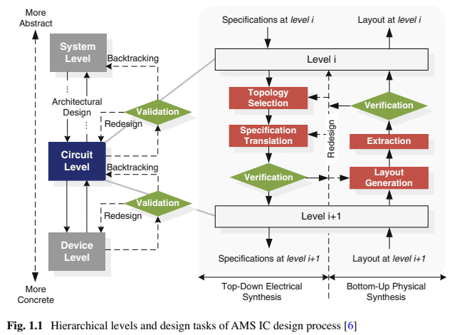
物理代写|模拟电路代写Analog Circuit代考|The AMS IC Design Flow
Even though most functions in today’s ICs are implemented using digital or digital signal processing circuitry, analog circuits are the link between digital circuitry and the continuous-valued external world [1-3]. In modern telecommunications and multimedia applications the integration of complex systems-on-a-chip (SoC) comprising analog or mixed-signal (AMS) blocks together with digital processors and memory blocks $[4,5]$ is a common practice.
Due to the continuous nature of the signal values handled by analog circuits, they are much more sensitive to noise and process variations than their digital counterpart, leading to a more complex and time demanding design. Hence, designers have been replacing most of analog circuits by digital computations, however, the following list enumerates some typical blocks referred as remaining analog forever [6]:
- On the input side of a system, the signals from a sensor, microphone or antenna must be sensed or received, amplified and filtered up to a level that allows digitalization with satisfying signal-to-noise and distortion ratio. Typical application of these circuits is in sensor interfaces, telecommunication receivers or sound recording;
- On the output side of a system, the signal from digital processing must be reconverted to analog and it has to be strengthened, so that it can drive outside load with low distortion. These circuits are typically used in telecommunication transmitters and loudspeakers;
- Mixed-signal circuits like sample-and-hold, analog-to-digital converters and frequency synthesizers. These blocks establish the interface between input/output sides of a system and digital processing parts of a SoC;
- Voltage or current reference circuits, and also, crystal oscillators, to offer stable and absolute references for the above mentioned circuitry;
- The last block of analog circuits are the high-performance digital circuits. The prime example is state-of-the-art microprocessors that are customized like AMS circuits, attempting to reach higher speed and lower power consumption.
物理代写|模拟电路代写Analog Circuit代考|Motivation for Analog Design Automation
In 1980 , analog ICs represented $32 \%$ of total IC shipments, that value increased to $49 \%$ in 2010 , and is forecast to grow to $57 \%$ of total IC shipments by 2018 [14]. These numbers are supported by the rampant growth in Medical/Health, automotive, LED lighting and energy management for buildings that make extensive use of electronic devices where AMS blocks are integrated in SoC designs. Despite the fact that analog blocks constitute only a small fraction of the components on a mixed-signal IC and SoC design, the design effort of analog components is considerably higher when compared to the digital ones, which is reflected in the total development time. Specifically, the development and test cost of AMS components usually surpasses the $50 \%$ of total design cost, even though the area occupied can be as low as $3 \%$ of the total SoC [15]. The three main reasons pointed for the larger development cycle of analog blocks are: the lack of effective CAD tools for electronic design automation (EDA); analog circuits are being integrated using technologies optimized for digital circuits; and, analog blocks are difficult to design and reuse because they are more sensitive to surrounding circuitry, environmental and process variations than their digital counterpart.
As stated, today’s analog design is supported by mature circuit simulators, layout editing environments and verification tools, however the design cycle for AMS ICs is still long and error-prone. These circuits suffer from diverse non-idealities and parasitic disturbances that, by not being considered in the early stages of development, are responsible for design errors and expensive redesign cycles, making them the bottleneck of SoC designs. Given the giant growth of AMS market, the economic pressure for high-quality yet cheap electronic products and time-to-market constraints, there is great pressure for new EDA tools to facilitate the life of analog designers, increasing their productivity and simultaneously improve the quality of resulting ICs. In fact, all design tasks of the AMS IC flow presented in Fig. $1.1$ have room for huge improvement in terms of user interaction, performance, and of course, automatic functionalities [15].
In the International Technology Roadmap for Semiconductors [5] the V-Cycle of a design summarizes the differences between analog and digital design automation, in particular, the implementation and the verification paths. The V-Cycle reveals that in the digital domain, EDA is fairly well developed and establish a low-level design process almost fully automated. The main gap in the digital design path of the system design are the tools and methodologies above the behavioral abstraction level. On the other hand, as the analog automation tools do not progress at the same pace of technology, knowledge and experience of the designer is always crucial for making decisions at all stages of the analog design flow. The “pushbutton” stage for analog design is still utopic and is historically a handcrafting process. EDA community has been primarily focused in the last decades on the evolution of the digital design automation methodologies to keep the pace with “More Moore” trend, featuring deep submicron technologies and multimillion transistor digital designs.
模拟电路代写
物理代写|模拟电路代写Analog Circuit 代考|Analog Topological Constraints
模拟布局的主要拓扑约束是设备匹配、设备对称性和设备接近度 [1], 如图 $2.1$ 所示。对称性将器件限制在 镜像位置, 用于抵消几何和电气问题, 并有助于降低对片上热梯度和两个相同信号流之间的寄生失配的敏感 性。匹配强制采用共同的栅极方向、共同的质心或器件之间的交叉数字化放置, 这通过进一步减少工艺引起 的不匹配对器件的影响来提高对称性的有益效果。邻近性将器件限制在特定位置, 因此它们可以共享一个八 共祇底/井区域, 被一个公共保护环包围, 也用于放置紧密匹配/对称的器件。通过确保片上接近, $[1,2]$. 用 于最大化模块之间距离的接近约束的变化在模拟布局设计中也很常见。
物理代写|模拟电路代写 Analog Circuit 代考|Floorplan Representations
在绝对表示中, 优化器明确移动单元, 因为每个单元都通过绝对坐标表示, 即制造网格, 这样, 可以描述每 个可能的放置。它被证明是实现拓扑约束最实用的解决方安, 因为它们可以最小化或直接使用坐标强制。然 而, 这种类型的表示允许在移动过程中出现非法重嗓 (例如, 单元格平移或旋转), 并且由于没有限制参考 单元格相对于另一个单元格的相对位置 (在某些情况下对称对除外) $\mathrm{a}$ 需要探索可行和不可行解决方案的巨 大搜索空间。
[3] 中报告了绝对坐标的首次使用。应用于模拟 IC 设计, 在 KOAN/ANAGRAM II [4] 中基于模拟退火 (SA) 的内核 [5], 详见第 1 节。 $2.1 .4$ 、用于最小化代价函数:
$$
\min f(x)=\alpha_1 f_1+\alpha_2 f_2(x)+\sum_i \alpha_i f_i(x)
$$
在哪里 $x$ 是设计变量向量 (即坐标, 如果允许的话, 每个单元格的旋转) 和 $\alpha$ 是权重向量。 $\mathrm{f} 1(x)$ 和 $\mathrm{f}_2(x)$ 是 需要最小化的两个主要/基本目标, 即放置区域和重叒 (其征罚成本不仅必须最小化, 而且在最终解决方安 中必须驱动为零, 即, $\mathrm{f}_2(x)=0$, 以获得允许的位置) 在单元格之间。其他 $\mathrm{fi}(x)$ 在单目标成本函数中同时 最小化目标, 例如平面图的纵横比、净长度的估计(通过伪生成树)、接近度和/或合并考虑因素。

物理代写|模拟电路代写Analog Circuit代考 请认准UprivateTA™. UprivateTA™为您的留学生涯保驾护航。
微观经济学代写
微观经济学是主流经济学的一个分支,研究个人和企业在做出有关稀缺资源分配的决策时的行为以及这些个人和企业之间的相互作用。my-assignmentexpert™ 为您的留学生涯保驾护航 在数学Mathematics作业代写方面已经树立了自己的口碑, 保证靠谱, 高质且原创的数学Mathematics代写服务。我们的专家在图论代写Graph Theory代写方面经验极为丰富,各种图论代写Graph Theory相关的作业也就用不着 说。
线性代数代写
线性代数是数学的一个分支,涉及线性方程,如:线性图,如:以及它们在向量空间和通过矩阵的表示。线性代数是几乎所有数学领域的核心。
博弈论代写
现代博弈论始于约翰-冯-诺伊曼(John von Neumann)提出的两人零和博弈中的混合策略均衡的观点及其证明。冯-诺依曼的原始证明使用了关于连续映射到紧凑凸集的布劳威尔定点定理,这成为博弈论和数学经济学的标准方法。在他的论文之后,1944年,他与奥斯卡-莫根斯特恩(Oskar Morgenstern)共同撰写了《游戏和经济行为理论》一书,该书考虑了几个参与者的合作游戏。这本书的第二版提供了预期效用的公理理论,使数理统计学家和经济学家能够处理不确定性下的决策。
微积分代写
微积分,最初被称为无穷小微积分或 “无穷小的微积分”,是对连续变化的数学研究,就像几何学是对形状的研究,而代数是对算术运算的概括研究一样。
它有两个主要分支,微分和积分;微分涉及瞬时变化率和曲线的斜率,而积分涉及数量的累积,以及曲线下或曲线之间的面积。这两个分支通过微积分的基本定理相互联系,它们利用了无限序列和无限级数收敛到一个明确定义的极限的基本概念 。
计量经济学代写
什么是计量经济学?
计量经济学是统计学和数学模型的定量应用,使用数据来发展理论或测试经济学中的现有假设,并根据历史数据预测未来趋势。它对现实世界的数据进行统计试验,然后将结果与被测试的理论进行比较和对比。
根据你是对测试现有理论感兴趣,还是对利用现有数据在这些观察的基础上提出新的假设感兴趣,计量经济学可以细分为两大类:理论和应用。那些经常从事这种实践的人通常被称为计量经济学家。
Matlab代写
MATLAB 是一种用于技术计算的高性能语言。它将计算、可视化和编程集成在一个易于使用的环境中,其中问题和解决方案以熟悉的数学符号表示。典型用途包括:数学和计算算法开发建模、仿真和原型制作数据分析、探索和可视化科学和工程图形应用程序开发,包括图形用户界面构建MATLAB 是一个交互式系统,其基本数据元素是一个不需要维度的数组。这使您可以解决许多技术计算问题,尤其是那些具有矩阵和向量公式的问题,而只需用 C 或 Fortran 等标量非交互式语言编写程序所需的时间的一小部分。MATLAB 名称代表矩阵实验室。MATLAB 最初的编写目的是提供对由 LINPACK 和 EISPACK 项目开发的矩阵软件的轻松访问,这两个项目共同代表了矩阵计算软件的最新技术。MATLAB 经过多年的发展,得到了许多用户的投入。在大学环境中,它是数学、工程和科学入门和高级课程的标准教学工具。在工业领域,MATLAB 是高效研究、开发和分析的首选工具。MATLAB 具有一系列称为工具箱的特定于应用程序的解决方案。对于大多数 MATLAB 用户来说非常重要,工具箱允许您学习和应用专业技术。工具箱是 MATLAB 函数(M 文件)的综合集合,可扩展 MATLAB 环境以解决特定类别的问题。可用工具箱的领域包括信号处理、控制系统、神经网络、模糊逻辑、小波、仿真等。