如果你也在 怎样代写数字硬件系统Digital Hardware System 这个学科遇到相关的难题,请随时右上角联系我们的24/7代写客服。嵌入式软件Embedded Software包括计算机的物理部分,如机箱、中央处理器(CPU)、随机存取存储器(RAM)、显示器、鼠标、键盘、计算机数据存储、显卡、声卡、扬声器和主板。
数字硬件系统Digital Hardware System 相比之下,软件是可由硬件存储和运行的指令集。硬件之所以被称为硬件,是因为它在变化方面是 “硬 “或僵化的,而软件是 “软 “的,因为它容易改变。硬件通常由软件指挥,执行任何命令或指令。硬件和软件的组合构成了一个可用的计算系统,尽管其他系统只存在硬件。
数字硬件系统Digital Hardware System代写,免费提交作业要求, 满意后付款,成绩80\%以下全额退款,安全省心无顾虑。专业硕 博写手团队,所有订单可靠准时,保证 100% 原创。最高质量的数字硬件系统Digital Hardware System作业代写,服务覆盖北美、欧洲、澳洲等 国家。 在代写价格方面,考虑到同学们的经济条件,在保障代写质量的前提下,我们为客户提供最合理的价格。 由于作业种类很多,同时其中的大部分作业在字数上都没有具体要求,因此数字硬件系统Digital Hardware System作业代写的价格不固定。通常在专家查看完作业要求之后会给出报价。作业难度和截止日期对价格也有很大的影响。
同学们在留学期间,都对各式各样的作业考试很是头疼,如果你无从下手,不如考虑my-assignmentexpert™!
my-assignmentexpert™提供最专业的一站式服务:Essay代写,Dissertation代写,Assignment代写,Paper代写,Proposal代写,Proposal代写,Literature Review代写,Online Course,Exam代考等等。my-assignmentexpert™专注为留学生提供Essay代写服务,拥有各个专业的博硕教师团队帮您代写,免费修改及辅导,保证成果完成的效率和质量。同时有多家检测平台帐号,包括Turnitin高级账户,检测论文不会留痕,写好后检测修改,放心可靠,经得起任何考验!
想知道您作业确定的价格吗? 免费下单以相关学科的专家能了解具体的要求之后在1-3个小时就提出价格。专家的 报价比上列的价格能便宜好几倍。
CS代写|数字硬件系统代写Digital Hardware System代考|CHIP LEVEL AND CIRCUIT BOARD-LEVEL DESIGN
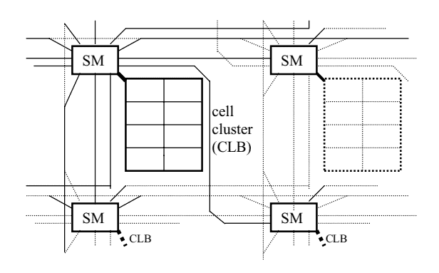
Circuit boards are used to mount the individual hardware building blocks (chips and others), to interconnect them, and to provide access to the interface signals via connectors. They also distribute the power and participate in removing the heat generated by the components. Larger digital systems are realized by several circuit boards mounted on ‘motherboards’ or in racks and cabinets. The circuit board simply constitutes the next hierarchical level of the hardware. As for the pin count of chips, it is desirable to have low signal counts at the external interfaces of a circuit board (the connectors). The design of the circuit boards can be so that they can easily be plugged together by means of connectors, or be performed by mapping several design modules to a single board. The main difference between the design levels of chip, board and cabinet design are in the degree of miniaturization and reliability and in the cost involved in designing application-specific systems and building them in a given volume. In contrast to the integrated circuits, boards are more expensive but easier to design, rely on a simpler manufacturing technology and can be used to implement low volume applications at reasonable costs. Still simpler yet more costly technology is required if an application-specific system can be plugged together from existing boards. If, however, the volume goes higher, it is more cost effective to map several boards to a single one, and multiple components to a single ASIC.
The design choices for a circuit board are similar to the ones for chip design. As in the case of the chips, a circuit board is a fixed, invariable hardware module. A circuit board design can be made so that different subsets of components can be supported and different components match with a compatible interface. The fixed hardware structure of a circuit board can be compensated by designing it to be configurable. Then it may allow more than one application or changes within an application without having to redesign the board. A standard circuit board serving many applications can be produced in higher volume (at lower cost), and its development costs become shared. Also the module interfaces at the chip and board levels are similar. It is e.g. common to link several boards via bus lines.
The interconnection of the chips is by fine leads on the surface of an epoxy carrier plane etched out from a copper coating. Circuit boards use between 1 and 12 interconnection planes fixed on top of each other. Leads at different planes are connected via connections (‘vias’) chemically deposited in small holes through the layers. It is common to use dedicated nonetched layers for the ground and power supply voltages. The integrated circuits are mounted to the top and bottom surfaces of the board. The placement of the components and the routing of the interconnection through the layers are done with the aid of CAD tools as in the case if chip design; for very simple boards, they can be done manually.
CS代写|数字硬件系统代写Digital Hardware System代考|Chip Versus Board-Level Design
It is possible to trade off chips level integration for board level integration to minimize the total cost. A circuit board can be collapsed into a single chip, but sometimes it can be more cost effective not to use a highly integrated chip but to distribute its functions to several chips (higher volume ones, or chips from different vendors).
The manufacturing costs of the circuit boards grow with the board area, with the number of layers, and the number of vias between the layers. For a simple board design, the integrated circuits should have as simple interfaces as possible (in terms of the number of i/o signals). This requirement is, of coarse, common to all modular structures (including software modules). For a single chip system the board design becomes almost trivial as, apart from simple support functions, only the external interface signals must be routed from the chip to appropriate connectors. System designs of this kind arise when a single-chip micro controller with integrated memory suffices to fulfill the processing requirements, or an FPGA configured from a serial EPROM.
This simplicity is not always achieved. If e.g. a processor chip needs a large external memory, a large number of interfacing signals is required. Current highly integrated chips have hundreds of interface signals. High pin counts require BGA packages that can no longer be supported by single or double layer circuit boards at all and hence raise the cost of the circuit board design even if just a subset of them is used for an application. An exception to the board costs increasing with the pin counts of the chips occurs when the layout of the pins of two chips to be connected to each other is so that they can be arranged side by side and the connections become short and are within a single board layer.
数字硬件系统代写
CS代写|数字硬件系统代写Digital Hardware System代考|CHIP LEVEL AND CIRCUIT BOARD-LEVEL DESIGN
电路板用于安装单个硬件构建块(芯片和其他),将它们互连,并通过连接器提供对接口信号的访问。他们还分配电力,并参与消除由组件产生的热量。较大的数字系统是通过安装在“主板”或机架和机柜中的几个电路板来实现的。电路板只是构成硬件的下一个层次。至于芯片的引脚数,希望在电路板的外部接口(连接器)具有低信号计数。电路板的设计可以使它们可以很容易地通过连接器连接在一起,或者通过将几个设计模块映射到单个电路板来执行。芯片、电路板和机柜设计的设计水平之间的主要区别在于小型化和可靠性的程度,以及设计特定应用系统和在给定体积内建造它们所涉及的成本。与集成电路相比,电路板更昂贵,但更容易设计,依赖于更简单的制造技术,可以以合理的成本实现小批量应用。如果一个特定应用的系统可以从现有的电路板上插入到一起,那么还需要更简单但更昂贵的技术。然而,如果体积增大,将多个板映射到单个板,将多个组件映射到单个ASIC,则更具成本效益。电路板的设计选择与芯片设计的选择类似。和芯片一样,电路板是一个固定不变的硬件模块。电路板设计可以支持不同的组件子集,并且不同的组件与兼容接口相匹配。电路板的固定硬件结构可以通过设计成可配置的来进行补偿。然后,它可以允许多个应用程序或应用程序内的更改,而不必重新设计板。服务于许多应用的标准电路板可以以更低的成本大批量生产,并且其开发成本可以共享。此外,模块接口在芯片和板的水平是相似的。通过公共汽车线路连接几块板是很常见的。芯片的互连是通过从铜涂层中蚀刻出来的环氧载体平面表面上的细导线实现的。电路板使用1到12个相互固定的互连平面。不同平面上的引线通过化学沉积在穿过层的小孔中的连接(“过孔”)连接。通常使用专用的非蚀刻层用于地面和电源电压。集成电路安装在电路板的顶部和底部表面。在芯片设计的情况下,在CAD工具的帮助下完成组件的放置和通过层的互连路由;对于非常简单的板,它们可以手工完成。
CS代写|数字硬件系统代写Digital Hardware System代考|Chip Versus Board-Level Design
这是可能的交易芯片级集成为板级集成,以尽量减少总成本。电路板可以压缩成一个芯片,但有时不使用高度集成的芯片,而是将其功能分配到几个芯片(容量较大的芯片,或来自不同供应商的芯片)会更经济有效。
电路板的制造成本随着电路板面积、层数和层间过孔数的增加而增长。对于一个简单的电路板设计,集成电路应该有尽可能简单的接口(就i/o信号的数量而言)。粗略地说,这个需求对于所有模块化结构(包括软件模块)来说都是通用的。对于单芯片系统,电路板设计变得几乎微不足道,除了简单的支持功能外,只有外部接口信号必须从芯片路由到适当的连接器。当带有集成存储器的单芯片微控制器足以满足处理要求,或者由串行EPROM配置的FPGA时,就会出现这种系统设计。
这种简单性并不总是能够实现。例如,如果一个处理器芯片需要一个大的外部存储器,就需要大量的接口信号。目前高度集成的芯片有数百个接口信号。高引脚数要求BGA封装不再支持单层或双层电路板,因此提高电路板设计的成本,即使只是其中的一个子集用于应用。电路板成本随着芯片引脚数的增加而增加的一个例外是,当两个芯片的引脚相互连接的布局是这样的,它们可以并排排列,连接变得很短,并且在一个电路板层内。

CS代写|数字硬件系统代写Digital Hardware System代考 请认准UprivateTA™. UprivateTA™为您的留学生涯保驾护航。
微观经济学代写
微观经济学是主流经济学的一个分支,研究个人和企业在做出有关稀缺资源分配的决策时的行为以及这些个人和企业之间的相互作用。my-assignmentexpert™ 为您的留学生涯保驾护航 在数学Mathematics作业代写方面已经树立了自己的口碑, 保证靠谱, 高质且原创的数学Mathematics代写服务。我们的专家在图论代写Graph Theory代写方面经验极为丰富,各种图论代写Graph Theory相关的作业也就用不着 说。
线性代数代写
线性代数是数学的一个分支,涉及线性方程,如:线性图,如:以及它们在向量空间和通过矩阵的表示。线性代数是几乎所有数学领域的核心。
博弈论代写
现代博弈论始于约翰-冯-诺伊曼(John von Neumann)提出的两人零和博弈中的混合策略均衡的观点及其证明。冯-诺依曼的原始证明使用了关于连续映射到紧凑凸集的布劳威尔定点定理,这成为博弈论和数学经济学的标准方法。在他的论文之后,1944年,他与奥斯卡-莫根斯特恩(Oskar Morgenstern)共同撰写了《游戏和经济行为理论》一书,该书考虑了几个参与者的合作游戏。这本书的第二版提供了预期效用的公理理论,使数理统计学家和经济学家能够处理不确定性下的决策。
微积分代写
微积分,最初被称为无穷小微积分或 “无穷小的微积分”,是对连续变化的数学研究,就像几何学是对形状的研究,而代数是对算术运算的概括研究一样。
它有两个主要分支,微分和积分;微分涉及瞬时变化率和曲线的斜率,而积分涉及数量的累积,以及曲线下或曲线之间的面积。这两个分支通过微积分的基本定理相互联系,它们利用了无限序列和无限级数收敛到一个明确定义的极限的基本概念 。
计量经济学代写
什么是计量经济学?
计量经济学是统计学和数学模型的定量应用,使用数据来发展理论或测试经济学中的现有假设,并根据历史数据预测未来趋势。它对现实世界的数据进行统计试验,然后将结果与被测试的理论进行比较和对比。
根据你是对测试现有理论感兴趣,还是对利用现有数据在这些观察的基础上提出新的假设感兴趣,计量经济学可以细分为两大类:理论和应用。那些经常从事这种实践的人通常被称为计量经济学家。
Matlab代写
MATLAB 是一种用于技术计算的高性能语言。它将计算、可视化和编程集成在一个易于使用的环境中,其中问题和解决方案以熟悉的数学符号表示。典型用途包括:数学和计算算法开发建模、仿真和原型制作数据分析、探索和可视化科学和工程图形应用程序开发,包括图形用户界面构建MATLAB 是一个交互式系统,其基本数据元素是一个不需要维度的数组。这使您可以解决许多技术计算问题,尤其是那些具有矩阵和向量公式的问题,而只需用 C 或 Fortran 等标量非交互式语言编写程序所需的时间的一小部分。MATLAB 名称代表矩阵实验室。MATLAB 最初的编写目的是提供对由 LINPACK 和 EISPACK 项目开发的矩阵软件的轻松访问,这两个项目共同代表了矩阵计算软件的最新技术。MATLAB 经过多年的发展,得到了许多用户的投入。在大学环境中,它是数学、工程和科学入门和高级课程的标准教学工具。在工业领域,MATLAB 是高效研究、开发和分析的首选工具。MATLAB 具有一系列称为工具箱的特定于应用程序的解决方案。对于大多数 MATLAB 用户来说非常重要,工具箱允许您学习和应用专业技术。工具箱是 MATLAB 函数(M 文件)的综合集合,可扩展 MATLAB 环境以解决特定类别的问题。可用工具箱的领域包括信号处理、控制系统、神经网络、模糊逻辑、小波、仿真等。