如果你也在 怎样代写数字硬件系统Digital Hardware System 这个学科遇到相关的难题,请随时右上角联系我们的24/7代写客服。嵌入式软件Embedded Software包括计算机的物理部分,如机箱、中央处理器(CPU)、随机存取存储器(RAM)、显示器、鼠标、键盘、计算机数据存储、显卡、声卡、扬声器和主板。
数字硬件系统Digital Hardware System 相比之下,软件是可由硬件存储和运行的指令集。硬件之所以被称为硬件,是因为它在变化方面是 “硬 “或僵化的,而软件是 “软 “的,因为它容易改变。硬件通常由软件指挥,执行任何命令或指令。硬件和软件的组合构成了一个可用的计算系统,尽管其他系统只存在硬件。
数字硬件系统Digital Hardware System代写,免费提交作业要求, 满意后付款,成绩80\%以下全额退款,安全省心无顾虑。专业硕 博写手团队,所有订单可靠准时,保证 100% 原创。最高质量的数字硬件系统Digital Hardware System作业代写,服务覆盖北美、欧洲、澳洲等 国家。 在代写价格方面,考虑到同学们的经济条件,在保障代写质量的前提下,我们为客户提供最合理的价格。 由于作业种类很多,同时其中的大部分作业在字数上都没有具体要求,因此数字硬件系统Digital Hardware System作业代写的价格不固定。通常在专家查看完作业要求之后会给出报价。作业难度和截止日期对价格也有很大的影响。
同学们在留学期间,都对各式各样的作业考试很是头疼,如果你无从下手,不如考虑my-assignmentexpert™!
my-assignmentexpert™提供最专业的一站式服务:Essay代写,Dissertation代写,Assignment代写,Paper代写,Proposal代写,Proposal代写,Literature Review代写,Online Course,Exam代考等等。my-assignmentexpert™专注为留学生提供Essay代写服务,拥有各个专业的博硕教师团队帮您代写,免费修改及辅导,保证成果完成的效率和质量。同时有多家检测平台帐号,包括Turnitin高级账户,检测论文不会留痕,写好后检测修改,放心可靠,经得起任何考验!
想知道您作业确定的价格吗? 免费下单以相关学科的专家能了解具体的要求之后在1-3个小时就提出价格。专家的 报价比上列的价格能便宜好几倍。
CS代写|数字硬件系统代写Digital Hardware System代考|Processors and Single-Chip Systems
The elementary Boolean gates with a few transistors only but individual inputs and outputs are not good candidates for a highly integrated standard chip without also integrating interconnection facilities (see section 2.2.4). If, however, a particular, complex Boolean function can be used in many applications (or in a system that is needed in very high volume), its integration makes sense. This is the case for the Boolean functions that implement the arithmetic operations on signed and unsigned binary numbers and floating point codes that are the building blocks in all numeric algorithms. If a complex function can be applied several times, one will try to reuse the same circuit with the aid of auxiliary select and control circuits. This gives rise to another important class of standard components or modules, the programmable processors.
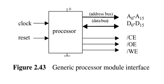
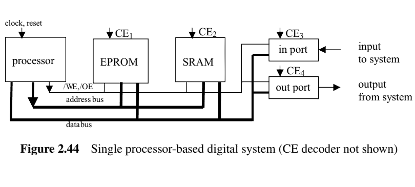
A processor chip integrates a multifunction circuit providing a number of complex Boolean functions (e.g., the arithmetic operations on 16-bit binary numbers) and a control circuit for the sequencing and the operand selection. In order to support many applications (each with its own sequence of operations and operand selections), it interfaces to a memory holding a list of operation codes (instructions) for the operations to be carried out. The same memory can also be used to store the operands. The interface to a generic processor chip or module is shown in Figure 2.43. It is complementary to the standard memory interface in Figure 2.35. The processor drives the address and control lines of the memory bus (to which a memory module is attached) to sequentially read instructions and operands and to write results. The bus can also be used to access input and output ports that are connected to it like memory chips using decoded chip enable signals. If the sequential execution of operations performed by the processor meets the performance requirements of an application, then the system can be as simple as shown in Figure 2.44.
The structure and the design of processors will be studied in much more detail in Chapters 4, 5, 6 and 8 . The most important attributes of a processor are the set of Boolean functions provided by it (in particular, the word size of the arithmetic operations) and the speed at which they can be executed. Commercial processor chips range from processors integrating a few thousand transistors and providing some 8-bit binary arithmetic and some other Boolean operations on 8-bit codes at a rate of a few million operations per second (MOPS) to processors executing arithmetic operations on 64-bit floating point codes at rates beyond a giga operations per second $(1 \mathrm{GOPS}=1000$ MOPS $)$ and employing more than $10^7$ transistors.
CS代写|数字硬件系统代写Digital Hardware System代考|Configurable Logic, FPGA
The individual CMOS gates and registers that are needed as building-blocks of applicationspecific computational circuits are not suitable to be packed as integrated chips as this approach cannot exploit the current level of integration. Instead, it is large inventories of such building blocks that are offered as chips with a provision to connect them in an application-specific way within the chip.
Even if most of the functions within a digital system are within highly integrated chips, there may remain some auxiliary ‘glue logic’ to interface them with each other, to decode selection signals for chips connected to a bus, or for some extra control and interface signals. A common choice is to implement such functions (except for bus and interface drivers) in a single or a few PLD devices (programmable logic device). PLD devices arrived in the 1980s as a replacement for the large variety of gate and registers functions used in small-scale integrated circuits before. They are multifunction circuits in which the selection signals of the actual function are generated on-chip. In the first PLD generations, the selection was defined once and for all by burning fuses within the silicon structure. Now these are generated by EEPROM cells that can be reprogrammed several times. The configuration memory and the transistor switches of a PLD add to its complexity, and any particular application will only use a part of its gates and flip-flops. As the PLD functions are usually just a small fraction of the overall digital system, these overheads are outweighed by the advantages of the higher integration of application specific functions and the possibility to change the circuit functions to some degree without changing the board design. PLD devices are programmed with bit streams that are compiled from a set of Boolean equations defining the desired behavior by design tools.
More specifically, PLD devices contain identical slices, each generating a signal that is defined by OR’ing a few (e.g., 8) AND terms computed from the input and output signals of the device and their complements, i.e. a low complexity disjunctive form, and optionally outputting their complements, or a registered signal by providing an integrated flip-flop (Figure 2.46). Output pins may be tri-stated and also serve as inputs. The AND terms are realized as wired AND functions and selected by means of a matrix of transistor switches. These switches and the output selectors are controlled by an on-chip non-volatile, electrically erasable memory. Thus the same PLD device can be configured for various functions including registers, feedback circuits using registers, decoders and selectors.
数字硬件系统代写
CS代写|数字硬件系统代写Digital Hardware System代考|Processors and Single-Chip Systems
只有几个晶体管但单独输入和输出的基本布尔门不适合高度集成的标准芯片,也不集成互连设施(见第2.2.4节)。但是,如果一个特定的复杂布尔函数可以在许多应用程序中使用(或者在需要非常大容量的系统中使用),那么它的集成是有意义的。这就是布尔函数的情况,布尔函数实现了对有符号和无符号二进制数和浮点码的算术运算,而浮点码是所有数字算法的构建块。如果一个复杂的功能可以多次应用,人们会尝试在辅助选择和控制电路的帮助下重复使用同一个电路。这就产生了另一类重要的标准元件或模块——可编程处理器。一个处理器芯片集成了一个多功能电路,该电路提供了一些复杂的布尔函数(例如,对16位二进制数的算术运算)和一个用于排序和操作数选择的控制电路。为了支持许多应用程序(每个应用程序都有自己的操作序列和操作数选择),它与存储要执行的操作代码(指令)列表的内存相连。同样的内存也可以用来存储操作数。通用处理器芯片或模块的接口如图2.43所示。它是图2.35中标准内存接口的补充。处理器驱动存储器总线的地址和控制线(存储器模块附着在其上),以顺序地读取指令和操作数并写入结果。总线也可以用来访问连接到它的输入和输出端口,就像使用解码芯片使能信号的存储芯片一样。如果处理器按顺序执行的操作能够满足应用程序的性能要求,则系统可以简单到如图2.44所示。处理器的结构和设计将在第4、5、6和8章中进行更详细的研究。处理器最重要的属性是它提供的一组布尔函数(特别是算术运算的字长)和它们的执行速度。商业处理器芯片的范围从集成了几千个晶体管并以每秒几百万次操作(MOPS)的速率在8位代码上提供一些8位二进制算术和一些其他布尔运算的处理器到以每秒超过千兆次操作的速率在64位浮点代码上执行算术运算的处理器$(1 \ maththrm {GOPS}=1000$ MOPS $)$和使用超过$10^7$晶体管。
CS代写|数字硬件系统代写Digital Hardware System代考|Configurable Logic, FPGA
作为特定应用计算电路的构建模块所需的单个CMOS门和寄存器不适合封装为集成芯片,因为这种方法无法利用当前的集成水平。相反,它是作为芯片提供的大量此类构建块,并提供在芯片内以特定于应用程序的方式连接它们的规定。
即使数字系统中的大部分功能都在高度集成的芯片中,也可能存在一些辅助的“粘合逻辑”来相互连接,解码连接到总线的芯片的选择信号,或用于一些额外的控制和接口信号。一种常见的选择是在一个或几个PLD设备(可编程逻辑设备)中实现这些功能(总线和接口驱动程序除外)。PLD器件于20世纪80年代问世,取代了之前在小型集成电路中使用的各种各样的门和寄存器功能。它们是多功能电路,其中实际功能的选择信号在片上产生。在第一代PLD中,选择是通过在硅结构内燃烧保险丝来一劳永逸地定义的。现在这些是由EEPROM单元产生的,可以被重新编程几次。配置存储器和晶体管开关的PLD增加了它的复杂性,任何特定的应用将只使用它的门和触发器的一部分。由于PLD功能通常只是整个数字系统的一小部分,这些开销被应用特定功能的更高集成度的优势和在某种程度上改变电路功能而不改变电路板设计的可能性所抵消。可编程逻辑器件是用比特流编程的,比特流是由一组布尔方程编译而成的,这些方程定义了设计工具所需的行为。
更具体地说,PLD器件包含相同的片,每个片产生一个信号,该信号由从器件的输入和输出信号及其补码(即低复杂度析取形式)计算的几个(例如8个)AND项定义,并可选地输出它们的补码,或者通过提供集成触发器(图2.46)输出一个寄存器信号。输出引脚可以是三态的,也可以作为输入。与项被实现为有线与函数,并通过晶体管开关矩阵来选择。这些开关和输出选择器由片上非易失性、电可擦除存储器控制。因此,相同的PLD器件可以配置用于各种功能,包括寄存器、使用寄存器的反馈电路、解码器和选择器。

CS代写|数字硬件系统代写Digital Hardware System代考 请认准UprivateTA™. UprivateTA™为您的留学生涯保驾护航。
微观经济学代写
微观经济学是主流经济学的一个分支,研究个人和企业在做出有关稀缺资源分配的决策时的行为以及这些个人和企业之间的相互作用。my-assignmentexpert™ 为您的留学生涯保驾护航 在数学Mathematics作业代写方面已经树立了自己的口碑, 保证靠谱, 高质且原创的数学Mathematics代写服务。我们的专家在图论代写Graph Theory代写方面经验极为丰富,各种图论代写Graph Theory相关的作业也就用不着 说。
线性代数代写
线性代数是数学的一个分支,涉及线性方程,如:线性图,如:以及它们在向量空间和通过矩阵的表示。线性代数是几乎所有数学领域的核心。
博弈论代写
现代博弈论始于约翰-冯-诺伊曼(John von Neumann)提出的两人零和博弈中的混合策略均衡的观点及其证明。冯-诺依曼的原始证明使用了关于连续映射到紧凑凸集的布劳威尔定点定理,这成为博弈论和数学经济学的标准方法。在他的论文之后,1944年,他与奥斯卡-莫根斯特恩(Oskar Morgenstern)共同撰写了《游戏和经济行为理论》一书,该书考虑了几个参与者的合作游戏。这本书的第二版提供了预期效用的公理理论,使数理统计学家和经济学家能够处理不确定性下的决策。
微积分代写
微积分,最初被称为无穷小微积分或 “无穷小的微积分”,是对连续变化的数学研究,就像几何学是对形状的研究,而代数是对算术运算的概括研究一样。
它有两个主要分支,微分和积分;微分涉及瞬时变化率和曲线的斜率,而积分涉及数量的累积,以及曲线下或曲线之间的面积。这两个分支通过微积分的基本定理相互联系,它们利用了无限序列和无限级数收敛到一个明确定义的极限的基本概念 。
计量经济学代写
什么是计量经济学?
计量经济学是统计学和数学模型的定量应用,使用数据来发展理论或测试经济学中的现有假设,并根据历史数据预测未来趋势。它对现实世界的数据进行统计试验,然后将结果与被测试的理论进行比较和对比。
根据你是对测试现有理论感兴趣,还是对利用现有数据在这些观察的基础上提出新的假设感兴趣,计量经济学可以细分为两大类:理论和应用。那些经常从事这种实践的人通常被称为计量经济学家。
Matlab代写
MATLAB 是一种用于技术计算的高性能语言。它将计算、可视化和编程集成在一个易于使用的环境中,其中问题和解决方案以熟悉的数学符号表示。典型用途包括:数学和计算算法开发建模、仿真和原型制作数据分析、探索和可视化科学和工程图形应用程序开发,包括图形用户界面构建MATLAB 是一个交互式系统,其基本数据元素是一个不需要维度的数组。这使您可以解决许多技术计算问题,尤其是那些具有矩阵和向量公式的问题,而只需用 C 或 Fortran 等标量非交互式语言编写程序所需的时间的一小部分。MATLAB 名称代表矩阵实验室。MATLAB 最初的编写目的是提供对由 LINPACK 和 EISPACK 项目开发的矩阵软件的轻松访问,这两个项目共同代表了矩阵计算软件的最新技术。MATLAB 经过多年的发展,得到了许多用户的投入。在大学环境中,它是数学、工程和科学入门和高级课程的标准教学工具。在工业领域,MATLAB 是高效研究、开发和分析的首选工具。MATLAB 具有一系列称为工具箱的特定于应用程序的解决方案。对于大多数 MATLAB 用户来说非常重要,工具箱允许您学习和应用专业技术。工具箱是 MATLAB 函数(M 文件)的综合集合,可扩展 MATLAB 环境以解决特定类别的问题。可用工具箱的领域包括信号处理、控制系统、神经网络、模糊逻辑、小波、仿真等。