如果你也在 怎样代写数字信号处理digital signal process这个学科遇到相关的难题,请随时右上角联系我们的24/7代写客服。数字信号处理digital signal process是指使用数字处理,如通过计算机或更专业的数字信号处理器,来进行各种信号处理操作。以这种方式处理的数字信号是一连串的数字,代表时间、空间或频率等领域中连续变量的样本。在数字电子学中,数字信号被表示为脉冲序列,它通常由晶体管的开关产生。
数字信号处理digital signal process和模拟信号处理是信号处理的子领域。DSP的应用包括音频和语音处理、声纳、雷达和其他传感器阵列处理、频谱密度估计、统计信号处理、数字图像处理、数据压缩、视频编码、音频编码、图像压缩、电信的信号处理、控制系统、生物医学工程和地震学等。
my-assignmentexpert™ 数字信号处理digital signal process作业代写,免费提交作业要求, 满意后付款,成绩80\%以下全额退款,安全省心无顾虑。专业硕 博写手团队,所有订单可靠准时,保证 100% 原创。my-assignmentexpert™, 最高质量的数字信号处理digital signal process作业代写,服务覆盖北美、欧洲、澳洲等 国家。 在代写价格方面,考虑到同学们的经济条件,在保障代写质量的前提下,我们为客户提供最合理的价格。 由于统计Statistics作业种类很多,同时其中的大部分作业在字数上都没有具体要求,因此数字信号处理digital signal process作业代写的价格不固定。通常在经济学专家查看完作业要求之后会给出报价。作业难度和截止日期对价格也有很大的影响。
想知道您作业确定的价格吗? 免费下单以相关学科的专家能了解具体的要求之后在1-3个小时就提出价格。专家的 报价比上列的价格能便宜好几倍。
my-assignmentexpert™ 为您的留学生涯保驾护航 在信息Information作业代写方面已经树立了自己的口碑, 保证靠谱, 高质且原创的数字信号处理digital signal process代写服务。我们的专家在信息Information代写方面经验极为丰富,各种数字信号处理digital signal process相关的作业也就用不着 说。
我们提供的数字信号处理digital signal process及其相关学科的代写,服务范围广, 其中包括但不限于:
调和函数 harmonic function
椭圆方程 elliptic equation
抛物方程 Parabolic equation
双曲方程 Hyperbolic equation
非线性方法 nonlinear method
变分法 Calculus of Variations
几何分析 geometric analysis
偏微分方程数值解 Numerical solution of partial differential equations
信号代写|数字信号处理作业代写digital signal process代考|Specifications
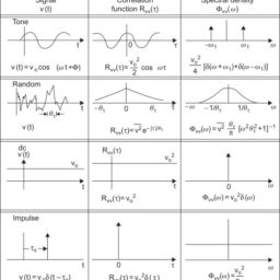
The definitions of resolution, total harmonic distortion (THD) and total harmonic distortion plus noise $(\mathrm{THD}+\mathrm{N})$ correspond to those for $\mathrm{AD}$ converters. Further specifications are discussed in the following.
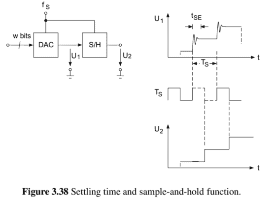
Settling Time. The time interval between transferring a binary word and achieving the analog output value within a specific error range is called the settling time $t_{S E}$. The settling time determines the maximum conversion frequency $f_{S_{\max }}=1 / t_{S E}$. Within this time, glitches between consecutive amplitude values can occur (see Fig. 3.38). With the help of a sample-and-hold circuit (deglitcher), the output voltage of the DA converter is sampled after the settling time and held.
信号代写|数字信号处理作业代写digital signal process代考|Switched Voltage and Current Sources
Switched Voltage Sources. The DA conversion with switched voltage sources shown in Fig. 3.43a is carried out with a reference voltage connected to a resistor network. The resistor network consists of $2^{w}$ resistors of equal resistance and is switched in stages to a binary-controlled decoder so that, at the output, a voltage $U_{2}$ is present corresponding to the input code. Figure $3.43 \mathrm{~b}$ shows the decoder for a 3-bit input code 101 .
Switched Current Sources. DA conversion with $2^{w}$ switched current sources is shown in Fig. 3.44. The decoder switches the corresponding number of current sources onto the current-voltage converter. The advantage of both techniques is the monotonicity which is guaranteed for ideal switches but also for slightly deviating resistances. The large number of resistors in switched current sources or the large number of switched current sources causes problems for long word-lengths. The techniques are used in combination with other methods for DA conversion of higher significant bits.
信号代写|数字信号处理作业代写digital signal process代考|Weighted Resistors and Capacitors
A reduction in the number of identical resistors or current sources is achieved with the following method.
Weighted Resistors. DA conversion with $w$ switched current sources which are weighted according to
$$
I_{1}=2 I_{2}=4 I_{3}=\cdots=2^{w-1} I_{w}
$$
is shown in Fig. 3.45. The output voltage is
$$
U_{2}=-R \cdot I=-R \cdot\left(b_{1} I_{1} 2^{0}+b_{2} I_{2} 2^{1}+b_{3} I_{3} 2^{2}+\cdots+b_{w} I_{w} 2^{w-1}\right)
$$
where $b_{n}$ takes values 0 or 1 . The implementation of DA conversion with switched current sources is carried out with weighted resistors as shown in Fig. 3.46. The output voltage is
$$
\begin{aligned}
U_{2} &=R \cdot I=R\left(\frac{b_{1}}{2 R}+\frac{b_{2}}{4 R}+\frac{b_{4}}{8 R}+\cdots+\frac{b_{w}}{2^{w} R}\right) U_{R} \
&=\left(b_{1} 2^{-1}+b_{2} 2^{-2}+b_{3} 2^{-3}+\cdots+b_{w} 2^{-w}\right) U_{R}
\end{aligned}
$$
数字信号处理代写
信号代写|数字信号处理作业代写DIGITAL SIGNAL PROCESS代考|SPECIFICATIONS
分辨率、总谐波失真的定义吨HD和总谐波失真加噪声(吨HD+ñ)对应于那些一种D转换器。进一步的规范将在下面讨论。
稳定时间。从传输一个二进制字到达到特定误差范围内的模拟输出值之间的时间间隔称为建立时间吨小号和. 建立时间决定了最大转换频率F小号最大限度=1/吨小号和. 在这段时间内,可能会出现连续幅度值之间的毛刺s和和F一世G.3.38. 在采样保持电路的帮助下d和Gl一世吨CH和r,DA转换器的输出电压在建立时间后被采样并保持。
信号代写|数字信号处理作业代写DIGITAL SIGNAL PROCESS代考|SWITCHED VOLTAGE AND CURRENT SOURCES
开关电压源。图 3.43a 所示的开关电压源的 DA 转换是通过连接到电阻网络的参考电压进行的。电阻网络由2在电阻相等的电阻,并分阶段切换到二进制控制的解码器,以便在输出端,电压在2存在对应于输入代码。数字3.43 b显示了 3 位输入代码 101 的解码器。
开关电流源。DA转换与2在开关电流源如图 3.44 所示。解码器将相应数量的电流源切换到电流电压转换器。这两种技术的优点是单调性,这对理想开关和稍微偏离的电阻都有保证。开关电流源中的大量电阻器或大量开关电流源会导致长字长问题。这些技术与其他方法结合使用,用于更高有效位的 DA 转换。
信号代写|数字信号处理作业代写DIGITAL SIGNAL PROCESS代考|WEIGHTED RESISTORS AND CAPACITORS
使用以下方法可以减少相同电阻器或电流源的数量。
加权电阻。DA转换与在被加权的开关电流源
一世1=2一世2=4一世3=⋯=2在−1一世在
如图 3.45 所示。输出电压为
在2=−R⋅一世=−R⋅(b1一世120+b2一世221+b3一世322+⋯+b在一世在2在−1)
在哪里bn取值 0 或 1 。使用图 3.46 所示的加权电阻器执行开关电流源的 DA 转换。输出电压为
在2=R⋅一世=R(b12R+b24R+b48R+⋯+b在2在R)在R =(b12−1+b22−2+b32−3+⋯+b在2−在)在R

信号代写|数字信号处理作业代写digital signal process代考 请认准UprivateTA™. UprivateTA™为您的留学生涯保驾护航。