如果你也在 怎样代写数字信号处理digital signal process这个学科遇到相关的难题,请随时右上角联系我们的24/7代写客服。数字信号处理digital signal process是指使用数字处理,如通过计算机或更专业的数字信号处理器,来进行各种信号处理操作。以这种方式处理的数字信号是一连串的数字,代表时间、空间或频率等领域中连续变量的样本。在数字电子学中,数字信号被表示为脉冲序列,它通常由晶体管的开关产生。
数字信号处理digital signal process和模拟信号处理是信号处理的子领域。DSP的应用包括音频和语音处理、声纳、雷达和其他传感器阵列处理、频谱密度估计、统计信号处理、数字图像处理、数据压缩、视频编码、音频编码、图像压缩、电信的信号处理、控制系统、生物医学工程和地震学等。
my-assignmentexpert™ 数字信号处理digital signal process作业代写,免费提交作业要求, 满意后付款,成绩80\%以下全额退款,安全省心无顾虑。专业硕 博写手团队,所有订单可靠准时,保证 100% 原创。my-assignmentexpert™, 最高质量的数字信号处理digital signal process作业代写,服务覆盖北美、欧洲、澳洲等 国家。 在代写价格方面,考虑到同学们的经济条件,在保障代写质量的前提下,我们为客户提供最合理的价格。 由于统计Statistics作业种类很多,同时其中的大部分作业在字数上都没有具体要求,因此数字信号处理digital signal process作业代写的价格不固定。通常在经济学专家查看完作业要求之后会给出报价。作业难度和截止日期对价格也有很大的影响。
想知道您作业确定的价格吗? 免费下单以相关学科的专家能了解具体的要求之后在1-3个小时就提出价格。专家的 报价比上列的价格能便宜好几倍。
my-assignmentexpert™ 为您的留学生涯保驾护航 在信息Information作业代写方面已经树立了自己的口碑, 保证靠谱, 高质且原创的数字信号处理digital signal process代写服务。我们的专家在信息Information代写方面经验极为丰富,各种数字信号处理digital signal process相关的作业也就用不着 说。
我们提供的数字信号处理digital signal process及其相关学科的代写,服务范围广, 其中包括但不限于:
调和函数 harmonic function
椭圆方程 elliptic equation
抛物方程 Parabolic equation
双曲方程 Hyperbolic equation
非线性方法 nonlinear method
变分法 Calculus of Variations
几何分析 geometric analysis
偏微分方程数值解 Numerical solution of partial differential equations
信号代写|数字信号处理作业代写digital signal process代考|Specifications
In the following, the most important specifications for AD conversion are presented.
Resolution. The resolution for a given word-length $w$ of an AD converter determines the smallest amplitude
$$
x_{\min }=Q=x_{\max } 2^{-(w-1)},
$$
which is equal to the quantization step $Q$.
Conversion Time. The minimum sampling period $T_{S}=1 / f_{S}$ between two samples is called the conversion time.
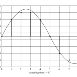
Sample-and-hold Circuit. Before quantization, the time-continuous function is sampled with the help of a sample-and-hold circuit, as shown in Fig. 3.24a.
The sampling period $T_{S}$ is divided into the sampling time $t_{S}$ in which the output voltage $U_{2}$ follows the input voltage $U_{1}$, and the hold time $t_{H}$. During the hold time the output voltage $U_{2}$ is constant and is converted into a binary word by quantization.
信号代写|数字信号处理作业代写digital signal process代考|Parallel Converter
Parallel Converter. A direct method for AD conversion is called parallel conversion (flash converter). In parallel converters, the output voltage of the sample-and-hold circuit is compared with a reference voltage $U_{R}$ with the help of $2^{w}-1$ comparators (see Fig. 3.29). The sample-and-hold circuit is controlled with sampling rate $f_{S}$ so that, during the hold time $t_{H}$, a constant voltage at the output of the sample-and-hold circuit is available. The outputs of the comparators are fed at sampling clock rate into a $\left(2^{w}-1\right)$-bit register and converted by a coding logic to a $w$-bit data word. This is fed at sampling clock rate to an output register. The sampling rates that can be achieved lie between 1 and $500 \mathrm{MHz}$ for a resolution of up to 10 bits. Owing to the large number of comparators, the technique is not feasible for high precision.
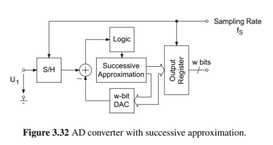
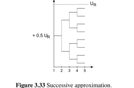
信号代写|数字信号处理作业代写digital signal process代考|Successive Approximation
AD converters with successive approximation consist of the functional modules shown in Fig. 3.32. The analog voltage is converted into a $w$-bit word within $w$ cycles. The converter consists of a comparator, a $w$-bit DA converter and logic for controlling the successive approximation.
The conversion process is explained with the help of Fig. 3.33. First, it is checked whether a positive or negative voltage is present at the comparator. If it is positive, the output $+0.5 U_{R}$ is fed to a DA converter to check whether the output voltage of the comparator is greater or less than $+0.5 U_{R}$. Then, the output of $(+0.5 \pm 0.25) U_{R}$ is fed to the DA comparator. The output of the comparator is then evaluated. This procedure is performed $w$ times and leads to a $w$-bit word.
For a resolution of 12 bits, sampling rates of up to $1 \mathrm{MHz}$ can be achieved. Higher resolutions of more than 16 bits are possible at a lower sampling rates.
数字信号处理代写
信号代写|数字信号处理作业代写DIGITAL SIGNAL PROCESS代考|SPECIFICATIONS
下面将介绍 AD 转换的最重要规范。
解析度。给定字长的分辨率在AD转换器的确定最小幅度
X分钟=问=X最大限度2−(在−1),
等于量化步长问.
转换时间。最小采样周期吨小号=1/F小号两个样本之间的时间称为转换时间。
采样保持电路。在量化之前,时间连续函数在采样保持电路的帮助下被采样,如图 3.24a 所示。
采样周期吨小号分为采样时间吨小号其中输出电压在2跟随输入电压在1, 和保持时间吨H. 在保持时间的输出电压在2是常数,并通过量化转换为二进制字。
信号代写|数字信号处理作业代写DIGITAL SIGNAL PROCESS代考|PARALLEL CONVERTER
并行转换器。AD转换的直接方法称为并行转换Fl一种sHC这n在和r吨和r. 在并联转换器中,采样保持电路的输出电压与参考电压进行比较在R在…的帮助下2在−1比较器s和和F一世G.3.29. 采样保持电路由采样率控制F小号这样,在保持时间吨H,采样保持电路输出端的恒定电压是可用的。比较器的输出以采样时钟速率馈送到一个(2在−1)位寄存器并由编码逻辑转换为在位数据字。这以采样时钟速率馈送到输出寄存器。可以达到的采样率介于 1 和500米H和分辨率高达 10 位。由于比较器数量众多,该技术不适用于高精度。
信号代写|数字信号处理作业代写DIGITAL SIGNAL PROCESS代考|SUCCESSIVE APPROXIMATION
具有逐次逼近的 AD 转换器由图 3.32 所示的功能模块组成。模拟电压被转换为在-位字内在循环。该转换器由一个比较器,一个在位 DA 转换器和用于控制逐次逼近的逻辑。
转换过程在图 3.33 的帮助下进行解释。首先,检查比较器上是否存在正电压或负电压。如果为正,则输出+0.5在R被馈送到DA转换器以检查比较器的输出电压是否大于或小于+0.5在R. 然后,输出(+0.5±0.25)在R被馈送到DA比较器。然后评估比较器的输出。执行此过程在次并导致在位字。
对于 12 位的分辨率,采样率高达1米H和可以实现。在较低的采样率下,超过 16 位的更高分辨率是可能的。

信号代写|数字信号处理作业代写digital signal process代考 请认准UprivateTA™. UprivateTA™为您的留学生涯保驾护航。