如果你也在 怎样代写数字电路DIGITAL CIRCUIT这个学科遇到相关的难题,请随时右上角联系我们的24/7代写客服。数字电路DIGITAL CIRCUIT是电子学的一个领域,涉及数字信号的研究和使用或产生数字信号的设备工程。这与模拟电子学和模拟信号相反。
数字电路DIGITAL CIRCUIT电路通常由逻辑门的大型组件制成,通常被封装在集成电路中。复杂的设备可能有简单的布尔逻辑功能的电子表示。
my-assignmentexpert™ 数字电路DIGITAL CIRCUIT作业代写,免费提交作业要求, 满意后付款,成绩80\%以下全额退款,安全省心无顾虑。专业硕 博写手团队,所有订单可靠准时,保证 100% 原创。my-assignmentexpert™, 最高质量的数字电路DIGITAL CIRCUIT作业代写,服务覆盖北美、欧洲、澳洲等 国家。 在代写价格方面,考虑到同学们的经济条件,在保障代写质量的前提下,我们为客户提供最合理的价格。 由于统计Statistics作业种类很多,同时其中的大部分作业在字数上都没有具体要求,因此数字电路DIGITAL CIRCUIT作业代写的价格不固定。通常在经济学专家查看完作业要求之后会给出报价。作业难度和截止日期对价格也有很大的影响。
想知道您作业确定的价格吗? 免费下单以相关学科的专家能了解具体的要求之后在1-3个小时就提出价格。专家的 报价比上列的价格能便宜好几倍。
my-assignmentexpert™ 为您的留学生涯保驾护航 在信息Information作业代写方面已经树立了自己的口碑, 保证靠谱, 高质且原创的数字电路DIGITAL CIRCUIT代写服务。我们的专家在信息Information代写方面经验极为丰富,各种数字电路DIGITAL CIRCUIT相关的作业也就用不着 说。
我们提供的数字电路DIGITAL CIRCUIT及其相关学科的代写,服务范围广, 其中包括但不限于:
调和函数 harmonic function
椭圆方程 elliptic equation
抛物方程 Parabolic equation
双曲方程 Hyperbolic equation
非线性方法 nonlinear method
变分法 Calculus of Variations
几何分析 geometric analysis
偏微分方程数值解 Numerical solution of partial differential equations
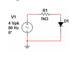
信号代写|数字电路作业代写digital circuit代考|LIMITER OR CLIPPING CIRCUIT
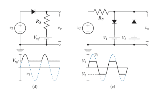
Diodes are often used in waveshaping applications. In particular, when used with a DC voltage in series with the diode, the output signal can be limited to the reference voltage level of the DC voltage source. Examples of clipping circuits are shown in Figure 2.13.
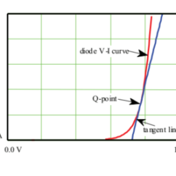
The simplified forward bias diode model of Figure $2.11$ can be used to analyze clipping circuits.
The circuit of Figure $2.13$ a will be used as an example of this analysis. When the input voltage $v_{i} \leq V_{d}+V_{r e f}$, the diode is reverse biased (or OFF). ${ }^{7}$ Therefore, the diode can be thought of as an open circuit. The output voltage in this case follows the input voltage,
$$
v_{o}=v_{i} .
$$
When the voltage $v_{i}>V_{d}+V_{\text {ref }}$, the diode is forward biased (or ON). Using the piece-wise linear model of the forward biased diode, a simplified equivalent circuit of the clipping circuit of Figure 2.13a is developed in Figure 2.14.
The output voltage $v_{o}$ of the clipping circuit when the diode is forward biased is found by analyzing the circuit in Figure $2.14$ using superposition and voltage division,
$$
v_{o}=\frac{r_{d}}{R_{s}+r_{d}} v_{i}+\frac{R_{s}}{R_{s}+r_{d}}\left(V_{d}+V_{r e f}\right) .
$$
信号代写|数字电路作业代写digital circuit代考|HALF-WAVE RECTIFIERS
One of the most common diode applications is the conversion of power from AC to DC for use as power supplies. Today’s power supplies involve sophisticated design principles that will be detailed in Chapter 14 (Book 4) in the fourth book of this series. However, the basic principles of converting from AC to DC power can be explored in this section.
Figure $2.18$ shows a half-wave rectifier circuit. The circuit is so named because it only allows current from the positive half cycle of the input to flow through the load resistor, $R$. Figure $2.18$ is identical to the clipping circuit of Figure $2.13 \mathrm{~d}$ with zero reference voltage.
If $v_{i}$ is a sinusoidal voltage with peak voltage $V_{m}$ and radian frequency $\omega$,
$$
v_{i}(t)=V_{m} \sin \omega t
$$
the average voltage $V_{d c}$ across the load, $R$, is
$$
V_{d c}=\frac{1}{T} \int_{0}^{T} v_{o}(t) d t
$$
where $T$ is the period of the sinusoid.
信号代写|数字电路作业代写DIGITAL CIRCUIT代考|FULL-WAVE RE
To remove the ripple from the output of a half-wave rectifier may require a very large capacitance. In many instances, the capacitor required to reduce the ripple on the half-wave rectified output voltage to the desired design specification may be prohibitively large.
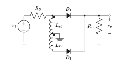
A full-wave rectifier circuit can be used as a more efficient way to reduce ripple on the output voltage. A center-tapped input transformer-coupled full-wave rectifier is shown in Figure 2.21. Each half of the transformer with the associated diode acts as a half-wave rectifier. The diode $\mathrm{D} 1$ conducts when the input $v_{i}>V_{\gamma}$ and $\mathrm{D} 2$ conducts when the input $v_{i}<V_{\gamma}$. Note that the secondary winding is capable of providing twice the voltage drop across the load resistor. Additionally, the input to the diodes and the output share a common ground between the load resistor and the center-tap.
数字电路代写
信号代写|数字电路作业代写DIGITAL CIRCUIT代考|LIMITER OR CLIPPING CIRCUIT
二极管通常用于波形整形应用。特别地,当使用与二极管串联的直流电压时,输出信号可以被限制为直流电压源的参考电压电平。限幅电路的例子如图 2.13 所示。
图的简化正向偏置二极管模型2.11可用于分析削波电路。
图的电路2.13a 将用作此分析的示例。当输入电压在一世≤在d+在r和F,二极管反向偏置这r这FF. 7因此,二极管可以被认为是开路。在这种情况下,输出电压跟随输入电压,
在这=在一世.
当电压在一世>在d+在参考 ,二极管正向偏置这r这ñ. 使用正向偏置二极管的分段线性模型,图 2.13a 的限幅电路的简化等效电路如图 2.14 所示。
输出电压在这二极管正向偏置时的削波电路通过分析图1中的电路得到2.14使用叠加和分压,
在这=rdRs+rd在一世+RsRs+rd(在d+在r和F).
信号代写|数字电路作业代写DIGITAL CIRCUIT代考|HALF-WAVE RECTIFIERS
最常见的二极管应用之一是将电源从交流电转换为直流电以用作电源。当今的电源涉及复杂的设计原则,将在第 14 章中详细介绍乙这这ķ4在本系列的第四本书中。但是,本节可以探讨从交流电转换为直流电的基本原理。
数字2.18显示了一个半波整流电路。该电路之所以如此命名,是因为它只允许来自输入正半周的电流流过负载电阻,R. 数字2.18与图的削波电路相同2.13 d与零参考电压。
如果在一世是具有峰值电压的正弦电压在米和弧度频率ω,
在一世(吨)=在米罪ω吨
平均电压在dC跨越负载,R, 是在dC=1吨∫0吨在这(吨)d吨
在哪里吨是正弦曲线的周期。
信号代写|数字电路作业代写DIGITAL CIRCUIT代考|FULL-WAVE RE
要消除半波整流器输出的纹波,可能需要非常大的电容。在许多情况下,将半波整流输出电压上的纹波降低到所需的设计规范所需的电容器可能非常大。
全波整流器电路可用作降低输出电压纹波的更有效方式。中心抽头输入变压器耦合全波整流器如图 2.21 所示。带有相关二极管的变压器的每一半充当半波整流器。二极管D1当输入时进行在一世>在C和D2当输入时进行在一世<在C. 请注意,次级绕组能够在负载电阻上提供两倍的电压降。此外,二极管的输入和输出在负载电阻和中心抽头之间共用一个接地。

信号代写|数字电路作业代写DIGITAL CIRCUIT代考 请认准UprivateTA™. UprivateTA™为您的留学生涯保驾护航。