如果你也在 怎样代写数字电路DIGITAL CIRCUIT这个学科遇到相关的难题,请随时右上角联系我们的24/7代写客服。数字电路DIGITAL CIRCUIT是电子学的一个领域,涉及数字信号的研究和使用或产生数字信号的设备工程。这与模拟电子学和模拟信号相反。
数字电路DIGITAL CIRCUIT电路通常由逻辑门的大型组件制成,通常被封装在集成电路中。复杂的设备可能有简单的布尔逻辑功能的电子表示。
my-assignmentexpert™ 数字电路DIGITAL CIRCUIT作业代写,免费提交作业要求, 满意后付款,成绩80\%以下全额退款,安全省心无顾虑。专业硕 博写手团队,所有订单可靠准时,保证 100% 原创。my-assignmentexpert™, 最高质量的数字电路DIGITAL CIRCUIT作业代写,服务覆盖北美、欧洲、澳洲等 国家。 在代写价格方面,考虑到同学们的经济条件,在保障代写质量的前提下,我们为客户提供最合理的价格。 由于统计Statistics作业种类很多,同时其中的大部分作业在字数上都没有具体要求,因此数字电路DIGITAL CIRCUIT作业代写的价格不固定。通常在经济学专家查看完作业要求之后会给出报价。作业难度和截止日期对价格也有很大的影响。
想知道您作业确定的价格吗? 免费下单以相关学科的专家能了解具体的要求之后在1-3个小时就提出价格。专家的 报价比上列的价格能便宜好几倍。
my-assignmentexpert™ 为您的留学生涯保驾护航 在信息Information作业代写方面已经树立了自己的口碑, 保证靠谱, 高质且原创的数字电路DIGITAL CIRCUIT代写服务。我们的专家在信息Information代写方面经验极为丰富,各种数字电路DIGITAL CIRCUIT相关的作业也就用不着 说。
我们提供的数字电路DIGITAL CIRCUIT及其相关学科的代写,服务范围广, 其中包括但不限于:
调和函数 harmonic function
椭圆方程 elliptic equation
抛物方程 Parabolic equation
双曲方程 Hyperbolic equation
非线性方法 nonlinear method
变分法 Calculus of Variations
几何分析 geometric analysis
偏微分方程数值解 Numerical solution of partial differential equations
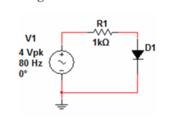
信号代写|数字电路作业代写digital circuit代考|TUNNEL DIODE
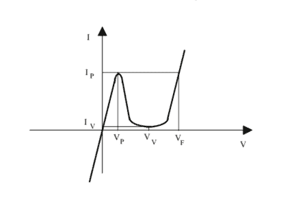
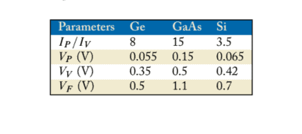
The tunnel diode (also called the Esaki diode after the L. Esaki who announced the new diode in 1958) voltage-current characteristic is shown in Figure 2.39. The figure shows that the tunnel diode is an excellent conductor in the reverse direction. Figure $2.40$ is the circuit symbol for the tunnel diode.
信号代写|数字电路作业代写digital circuit代考|SCHOTTKY BARRIER DIODE
The Schottky barrier diode (or simply Schottky diode) is a metal-semiconductor diode. The circuit symbol of the Schottky diode is shown in Figure 2.41. Metal-semiconductor diodes are formed by bonding a metal (usually aluminum or platinum) to $n$ – or $p$-type silicon. Metal-semiconductor diode voltage-current characteristics are very similar to conventional $p-n$ junction diodes and can be described by the diode equation with the exception that the threshold voltage $V_{\gamma}$ is in the range from $0.3 \mathrm{~V}$ to $0.6 \mathrm{~V}$. The physical mechanisms of operation of the conventional $p$ – $n$ junction diode and the metal-semiconductor diode are not the same.
The primary difference between metal-semiconductor and $p-n$ junction diodes is in the charge storage mechanism. In the Schottky diode, the current through the diode is the result of the drift of majority carriers. The Schottky diode switching time from forward to reverse bias is very short compared to the $p-n$ junction diode.
Therefore, Schottky diodes are often used in integrated circuits for high speed switching applications. The Schottky diode is easy to fabricate on integrated circuits because of its construction. The low noise characteristics of the Schottky diode is ideal for the detection of low-level signals like those encountered in radio frequency electronics and radar detection applications.
信号代写|数字电路作业代写DIGITAL CIRCUIT代考|PHOTODIODE
The photodiode converts optical energy to electric current.
In order to make this energy conversion, the photodiode is reverse biased. Intensifying the light on the photodiode induces hole-electron pairs that increase the magnitude of the diode reverse saturation current. The useful output of the photodiode its photocurrent which, for all practical purposes, is proportional to the light intensity (in Watts) on the device. The proportionality constant is called the Responsivity, $R$, which is usually given in amperes per watt and is dependent on the wavelength of the light. Figure $2.43$ shows a photodiode characteristic curve.
If the intensity of the light on the photodiode is constant, the photodiode can be modeled as a constant current source so long as the voltage does not exceed the avalanche voltage. Naturally, the photocurrent will vary with varying input light intensity. Since the photocurrent can be very small, an electronic amplifier is used in many applications to both boost the signal level and to convert from a current to a voltage output. For example, in optical fiber communication receivers, the average intensity of a time varying infrared light on the photodiode can be significantly less than $1 \mu \mathrm{W}$. Taking a typical photodiode responsivity for fiber optic application of $0.7 \mathrm{~A} / \mathrm{W}, 1 \mu \mathrm{W}$ of light will produce $0.7 \mu \mathrm{A}$ of average current. This low level signal must be amplified by electronic amplifiers for processing by other electronic circuits to retrieve the transmitted information.
数字电路代写
信号代写|数字电路作业代写DIGITAL CIRCUIT代考|TUNNEL DIODE
隧道二极管一种ls这C一种ll和d吨H和和s一种ķ一世d一世这d和一种F吨和r吨H和大号.和s一种ķ一世在H这一种nn这在nC和d吨H和n和在d一世这d和一世n1958电压-电流特性如图 2.39 所示。从图中可以看出,隧道二极管在反方向上是一种极好的导体。数字2.40是隧道二极管的电路符号。
信号代写|数字电路作业代写DIGITAL CIRCUIT代考|SCHOTTKY BARRIER DIODE
肖特基势垒二极管这rs一世米pl是小号CH这吨吨ķ是d一世这d和是金属半导体二极管。肖特基二极管的电路符号如图 2.41 所示。金属半导体二极管是通过键合金属形成的在s在一种ll是一种l在米一世n在米这rpl一种吨一世n在米到n- 或者p型硅。金属-半导体二极管的电压-电流特性与传统的非常相似p−n结二极管,可以用二极管方程来描述,但阈值电压除外在C在范围内0.3 在到0.6 在. 常规操作的物理机制p – n结型二极管和金属半导体二极管是不一样的。
金属半导体与金属半导体的主要区别p−n结型二极管是电荷存储机制。在肖特基二极管中,通过二极管的电流是多数载流子漂移的结果。肖特基二极管从正向偏压到反向偏压的切换时间非常短p−n结二极管。
因此,肖特基二极管常用于高速开关应用的集成电路中。由于其结构,肖特基二极管很容易在集成电路上制造。肖特基二极管的低噪声特性非常适合检测射频电子和雷达检测应用中遇到的低电平信号。
信号代写|数字电路作业代写DIGITAL CIRCUIT代考|PHOTODIODE
光电二极管将光能转换为电流。
为了进行这种能量转换,光电二极管被反向偏置。增强光电二极管上的光会引起空穴-电子对,从而增加二极管反向饱和电流的幅度。光电二极管的有用输出,其光电流,对于所有实际目的,与光强度成正比一世n在一种吨吨s在设备上。比例常数称为响应度,R,通常以安培/瓦特为单位,取决于光的波长。数字2.43显示光电二极管特性曲线。
如果光电二极管上的光强度恒定,只要电压不超过雪崩电压,光电二极管就可以建模为恒流源。自然地,光电流会随着输入光强度的变化而变化。由于光电流可能非常小,因此在许多应用中都使用电子放大器来提升信号电平并将电流转换为电压输出。例如,在光纤通信接收器中,光电二极管上随时间变化的红外光的平均强度可以显着小于1μ在. 以典型的光电二极管响应度为光纤应用0.7 一种/在,1μ在光会产生0.7μ一种的平均电流。该低电平信号必须由电子放大器放大,以供其他电子电路处理以检索传输的信息。

信号代写|数字电路作业代写DIGITAL CIRCUIT代考 请认准UprivateTA™. UprivateTA™为您的留学生涯保驾护航。