如果你也在 怎样代写电路设计Intro to circuit design这个学科遇到相关的难题,请随时右上角联系我们的24/7代写客服。电路设计Intro to circuit design一个简单的电路由电阻器、电容器、电感器、晶体管、二极管和集成电路组成。这些基本的电子元件是由导电线连接的。电流可以很容易地在这些导线之间流动,以便使电子元件处于工作状态。
电路设计Intro to circuit design过程从规格书开始,规格书说明了成品设计必须提供的功能,但没有指出如何实现这些功能。最初的规格书基本上是对客户希望成品电路实现的技术上的详细描述,可以包括各种电气要求,如电路将接收什么信号,必须输出什么信号,有什么电源,允许消耗多少功率。规格书还可以(通常也是如此)设定设计必须满足的一些物理参数,如尺寸、重量、防潮性、温度范围、热输出、振动容限和加速度容限等。
my-assignmentexpert™ 电路设计Intro to circuit design作业代写,免费提交作业要求, 满意后付款,成绩80\%以下全额退款,安全省心无顾虑。专业硕 博写手团队,所有订单可靠准时,保证 100% 原创。my-assignmentexpert™, 最高质量的电路设计Intro to circuit design作业代写,服务覆盖北美、欧洲、澳洲等 国家。 在代写价格方面,考虑到同学们的经济条件,在保障代写质量的前提下,我们为客户提供最合理的价格。 由于统计Statistics作业种类很多,同时其中的大部分作业在字数上都没有具体要求,因此电路设计Intro to circuit design作业代写的价格不固定。通常在经济学专家查看完作业要求之后会给出报价。作业难度和截止日期对价格也有很大的影响。
想知道您作业确定的价格吗? 免费下单以相关学科的专家能了解具体的要求之后在1-3个小时就提出价格。专家的 报价比上列的价格能便宜好几倍。
my-assignmentexpert™ 为您的留学生涯保驾护航 在电子工程Electrical Engineering作业代写方面已经树立了自己的口碑, 保证靠谱, 高质且原创的电子工程Electrical Engineering代写服务。我们的专家在电路设计Intro to circuit design代写方面经验极为丰富,各种电路设计Intro to circuit design相关的作业也就用不着 说。
我们提供的电路设计Intro to circuit design及其相关学科的代写,服务范围广, 其中包括但不限于:
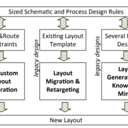
电子工程代写|电路设计作业代写Intro to circuit design代考|Existing Approaches to Analog IC Sizing Automation
Despite the overall lack of any well-established flow for analog IC design automation, the automation of analog circuit sizing using optimization is a quite established approach [1]. These tools for automatic IC sizing vary mostly by the optimization method they use and how they estimate the circuit’s performance, while in a manual design approach, the estimate can be done using approximate equations in early stages and using the circuit simulator in a later stage to verify and fine-tune the initial design.
For automatic sizing, simulation-based optimization is the most prevalent method in both industrial $[2,3]$ and academic $[4,5]$ environments, since designers prefer to avoid the risks of estimation errors in equation-based performance approximation. In fact, the trend in analog IC sizing automation is to increase performance estimation accuracy. The consideration of variability [6], models from electromagnetic simulation [7], and layout effects [8] to ensure that the optimization is done over a performance landscape that is as close as possible to the true performance of a fabricated prototype.
Nevertheless, instead of going from the target specification to the corresponding device’s sizes, the designer or the electronic design automation (EDA) tool is actually going from tentative devices’ sizes to the corresponding circuit performance countless times, trying combinations of design variables until a suitable sizing where the circuit meets specifications. While these EDA approaches are able to find solutions, and sometimes extremely effective ones, the long execution time while not the only is still major deterrent. More, since these approaches do not store the output of the tentative tries when a new design target appears, most of the data produced are not considered. Even the available previous designs, which sometimes are used to initialize new optimization runs, are not used to their full potential to predict effectively better starting points for the new optimization runs. Having identified this gap, and with the rise of the machine and deep learning, together with the increasing availability of computational resources and data, researchers started to explore new data-centric approaches. The next section presents some of these new approaches that are capable of predicting devices sizes, given some previous designs and new target specifications or technology node.
电子工程代写|电路设计作业代写Intro to circuit design代考|Machine Learning Applied to Sizing Automation
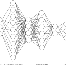
ML, and in particular artificial neural network (ANN) models, has been used in some works to address analog IC sizing automation. In [9], ANN models for estimating the performance parameters of complementary metal-oxide semiconductor (CMOS) operational amplifier topologies were presented. In addition, effective methods for the generation of training data and consequent use for training of the model were proposed to enhance the accuracy of the ANN models. The efficiency and accuracy of the performance results were then tested in a genetic algorithm-based circuit synthesis framework. This genetic synthesis tool optimizes a fitness function based on a set of performance constraints specified by the user. Finally, the performance parameters of the synthesized circuits were validated by SPICE simulations and later compared with those predicted by the ANN models. The set of test bench circuits presented in this work can be used to extract performance parameters from other op-amp topologies other than ones specifically studied here. Circuits with different functionalities than an op-amp would need new sets of SPICE test bench circuits to create appropriate ANN models.
The ANN models trained in this work used data generated from SPICE, where time-dependent and frequency-dependent data points were created for numerous circuit topologies instantiating the target op-amp. The training set was comprised of 3095 points, while the validation set was comprised of 1020 points. The neural network toolbox from MATLAB was used to simulate the networks. The structure of the network is simply comprised of an input layer, an output layer, and a single hidden layer. Different numbers of hidden layer nodes (from 8 to 14) were iteratively tested to obtain the best possible generalization and accuracy on both training and validation examples. The hyperbolic tangent sigmoid function was used as the activation function for all hidden layer nodes, and a linear function was used as the activation function for all output layer nodes. It should be noted that each network only has one single output node since a different network was designed to model each individual op-amp performance parameter. Collecting the data took approximately $1 \mathrm{~h} 47 \mathrm{~m}$, and generating all seven performances estimates using the ANN models took around $51.9 \mu \mathrm{s}$, which, when compared with using SPICE directly, resulted in a speedup factor of about 40,000 times. Still, the model is trained to replace the circuit simulator; $[10]$ takes a similar approach.
While the improvement in the optimization efficiency is remarkable, the loss in accuracy goes against the designers’ preferences preventing these, and other, performance approximation methods to establish themselves.
电路设计作业代写
电子工程代写|电路设计作业代写INTRO TO CIRCUIT DESIGN代考|EXISTING APPROACHES TO ANALOG IC SIZING AUTOMATION
尽管总体上缺乏任何成熟的模拟 IC 设计自动化流程,但使用优化的模拟电路尺寸自动化是一种相当成熟的方法1. 这些用于自动 IC 尺寸调整的工具主要取决于它们使用的优化方法以及它们如何估计电路的性能,而在手动设计方法中,可以在早期使用近似方程并在后期使用电路模拟器来完成估计验证和微调初始设计。
对于自动选型,基于仿真的优化是工业界最流行的方法。[2,3]和学术[4,5]环境,因为设计人员更愿意避免基于方程的性能近似中估计错误的风险。事实上,模拟 IC 尺寸自动化的趋势是提高性能估计精度。可变性的考虑6, 来自电磁仿真的模型7, 和布局效果8确保优化是在尽可能接近制造原型真实性能的性能环境中完成的。
然而,设计师或电子设计自动化不是从目标规格到相应设备的尺寸和D一种工具实际上是无数次地从暂定器件的尺寸到相应的电路性能,尝试设计变量的组合,直到电路符合规格的合适尺寸。虽然这些 EDA 方法能够找到解决方案,有时甚至是非常有效的解决方案,但较长的执行时间虽然不是唯一的,但仍然是主要的威慑。此外,由于这些方法在出现新的设计目标时不会存储试探性尝试的输出,因此不会考虑产生的大部分数据。即使是可用的先前设计(有时用于初始化新的优化运行)也没有充分发挥其潜力来有效地预测新优化运行的更好起点。确定了这一差距,随着机器和深度学习的兴起,随着计算资源和数据的可用性越来越高,研究人员开始探索以数据为中心的新方法。下一节介绍了其中一些能够预测设备尺寸的新方法,给定一些先前的设计和新的目标规范或技术节点。
电子工程代写|电路设计作业代写INTRO TO CIRCUIT DESIGN代考|MACHINE LEARNING APPLIED TO SIZING AUTOMATION
ML,尤其是人工神经网络一种ññ模型,已在一些工作中用于解决模拟 IC 尺寸自动化问题。在9, 用于估计互补金属氧化物半导体性能参数的人工神经网络模型C米这小号提出了运算放大器拓扑结构。此外,还提出了生成训练数据和随后用于模型训练的有效方法,以提高人工神经网络模型的准确性。然后在基于遗传算法的电路综合框架中测试性能结果的效率和准确性。该基因合成工具根据用户指定的一组性能约束优化适应度函数。最后,合成电路的性能参数通过 SPICE 仿真进行验证,然后与 ANN 模型预测的性能参数进行比较。这项工作中介绍的测试台电路集可用于从其他运算放大器拓扑中提取性能参数,而不是此处专门研究的拓扑。
在这项工作中训练的 ANN 模型使用从 SPICE 生成的数据,其中为实例化目标运算放大器的众多电路拓扑创建了时间相关和频率相关的数据点。训练集由 3095 个点组成,而验证集由 1020 个点组成。MATLAB 的神经网络工具箱用于模拟网络。网络的结构简单地由一个输入层、一个输出层和一个隐藏层组成。不同数量的隐藏层节点Fr这米8吨这14进行了迭代测试,以在训练和验证示例上获得最佳的泛化和准确性。双曲正切sigmoid函数被用作所有隐藏层节点的激活函数,线性函数被用作所有输出层节点的激活函数。应该注意的是,每个网络只有一个输出节点,因为设计了不同的网络来模拟每个单独的运算放大器性能参数。收集数据大约花了1 H47 米,并使用 ANN 模型生成所有七个性能估计值51.9μs,与直接使用 SPICE 相比,加速因子约为 40,000 倍。尽管如此,该模型还是被训练来代替电路模拟器;[10]采取类似的方法。
虽然优化效率的提高是显着的,但准确性的损失违背了设计者的偏好,从而阻止了这些以及其他性能近似方法的建立。

电子工程代写|电路设计作业代写Intro to circuit design代考 请认准UprivateTA™. UprivateTA™为您的留学生涯保驾护航。
电磁学代考
物理代考服务:
物理Physics考试代考、留学生物理online exam代考、电磁学代考、热力学代考、相对论代考、电动力学代考、电磁学代考、分析力学代考、澳洲物理代考、北美物理考试代考、美国留学生物理final exam代考、加拿大物理midterm代考、澳洲物理online exam代考、英国物理online quiz代考等。
光学代考
光学(Optics),是物理学的分支,主要是研究光的现象、性质与应用,包括光与物质之间的相互作用、光学仪器的制作。光学通常研究红外线、紫外线及可见光的物理行为。因为光是电磁波,其它形式的电磁辐射,例如X射线、微波、电磁辐射及无线电波等等也具有类似光的特性。
大多数常见的光学现象都可以用经典电动力学理论来说明。但是,通常这全套理论很难实际应用,必需先假定简单模型。几何光学的模型最为容易使用。
相对论代考
上至高压线,下至发电机,只要用到电的地方就有相对论效应存在!相对论是关于时空和引力的理论,主要由爱因斯坦创立,相对论的提出给物理学带来了革命性的变化,被誉为现代物理性最伟大的基础理论。
流体力学代考
流体力学是力学的一个分支。 主要研究在各种力的作用下流体本身的状态,以及流体和固体壁面、流体和流体之间、流体与其他运动形态之间的相互作用的力学分支。
随机过程代写
随机过程,是依赖于参数的一组随机变量的全体,参数通常是时间。 随机变量是随机现象的数量表现,其取值随着偶然因素的影响而改变。 例如,某商店在从时间t0到时间tK这段时间内接待顾客的人数,就是依赖于时间t的一组随机变量,即随机过程
Matlab代写
MATLAB 是一种用于技术计算的高性能语言。它将计算、可视化和编程集成在一个易于使用的环境中,其中问题和解决方案以熟悉的数学符号表示。典型用途包括:数学和计算算法开发建模、仿真和原型制作数据分析、探索和可视化科学和工程图形应用程序开发,包括图形用户界面构建MATLAB 是一个交互式系统,其基本数据元素是一个不需要维度的数组。这使您可以解决许多技术计算问题,尤其是那些具有矩阵和向量公式的问题,而只需用 C 或 Fortran 等标量非交互式语言编写程序所需的时间的一小部分。MATLAB 名称代表矩阵实验室。MATLAB 最初的编写目的是提供对由 LINPACK 和 EISPACK 项目开发的矩阵软件的轻松访问,这两个项目共同代表了矩阵计算软件的最新技术。MATLAB 经过多年的发展,得到了许多用户的投入。在大学环境中,它是数学、工程和科学入门和高级课程的标准教学工具。在工业领域,MATLAB 是高效研究、开发和分析的首选工具。MATLAB 具有一系列称为工具箱的特定于应用程序的解决方案。对于大多数 MATLAB 用户来说非常重要,工具箱允许您学习和应用专业技术。工具箱是 MATLAB 函数(M 文件)的综合集合,可扩展 MATLAB 环境以解决特定类别的问题。可用工具箱的领域包括信号处理、控制系统、神经网络、模糊逻辑、小波、仿真等。